E1M Carrier Board Design Guide
Release History
| Revision | Changes | Date |
|---|---|---|
| 0.1 |
| October 2026 |
| 0.2 |
| October 2026 |
| 0.3 |
| October 2026 |
| 0.4 |
| October 2026 |
| 0.5 |
| October 2026 |
| 0.6 |
| October 2026 |
| 0.7 |
| October 2026 |
| 0.8 |
| October 2026 |
| 0.9 |
| October 2026 |
1 Introduction
1.1 Purpose and Scope
This guide gives one set of carrier-board rules that works with every conformant module. A carrier built to it accepts any E1M™ module (35 × 35 mm, 312 pads) and, where the carrier uses the E1M-X™ footprint, any E1M-X module (45 × 65 mm, 496 pads). It is written for hardware engineers who design carrier boards, breakout boards and end products that mount a module.
The guide covers the carrier side of the interface: footprint and assembly, PCB stack-up, the 5 V input, the module output rails, I/O levels and back-powering, the control pins and sequencing, and every interface on the pinout. It does not cover:
- the internal design of any module (silicon, on-module parts, firmware);
- software: the Alp SDK™, device trees, Yocto and Zephyr builds;
- end-product certification (EMC, radio, safety), beyond the carrier rules that a certification depends on.
The E1M specification (footprint, pinout, electrical clauses and the pinout JSON) is an open standard, published under CC BY-SA 4.0 (E1M-STD §10.2). The modules are proprietary Alp Lab AB products; their schematics, layouts and firmware are not part of the standard and not part of this guide (E1M-STD §10.3).
1.2 Reference Modules
The rules in this guide are checked against the reference modules below. A future conformant module is covered by the same rules; its manifest and datasheet add only module-specific values.
| Item | E1M-AEN | E1M-X V2N | E1M-X V2N-M1 |
|---|---|---|---|
| Form factor | E1M, 35 × 35 mm, 312 pads | E1M-X, 45 × 65 mm, 496 pads | E1M-X, 45 × 65 mm, 496 pads |
| SKUs | E1M-AEN301, 401, 501, 601, 701, 801, 803 | E1M-V2N101, E1M-V2N102, E1M-V2N103 | E1M-V2M101, E1M-V2M102, E1M-V2M103 |
| Primary silicon | Alif Semiconductor Ensemble E3– E8 | Renesas RZ/V2N R9A09G056N44GBG#AC0 | Renesas RZ/V2N R9A09G056N44GBG#AC0 + DeepX DX-M1 |
| Hardware revision covered | R3 (DS-AEN-001 rev 0.20) | Not stated in DS-V2N-001 rev 0.14; held in the on-module identity EEPROM | Not stated in DS-V2N-M1-001 rev 0.17; held in the on-module identity EEPROM |
| Module documents | DS-AEN-001 0.21, HG-AEN-001 0.11 | DS-V2N-001 0.15, HG-V2N-001 0.7 | DS-V2N-M1-001 0.19, HG-V2N-M1-001 0.8 |
| Ambient operating temperature | − 40 to +75 °C | − 40 to +85 °C | − 40 to +85 °C |
E1M-AEN hardware revision R2 differs from R3 on carrier-visible pads (USB pads, SD_VDD direction, CSI-2 polarity, VIO_OUT current, 5 V window). This guide covers R3. Check a carrier against DS-AEN-001 "Hardware Revisions" before it carries an R2 module; Chapter 2 lists the hazards.
1.3 Document Hierarchy and Precedence
Four kinds of document describe a carrier. Figure 1 shows how they depend on each other.
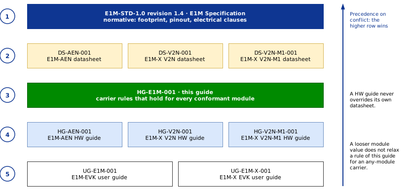
Document hierarchy and precedence
- E1M-STD-1.0 revision 1.4 is normative. It fixes the footprint, the pinout, and the carrier and module clauses in §6, §7 and §9.
- This guide (HG-E1M-001) turns the specification into carrier design rules and adds informative practice. Where one module's value is tighter than another's, the guide uses the tighter one.
- Module datasheets and hardware design guides (DS-AEN-001, HG-AEN-001, DS-V2N-001, HG-V2N-001, DS-V2N-M1-001, HG-V2N-M1-001) give the values and assembly options of one module family.
- EVK user guides (UG-E1M-001, UG-E1M-X-001) are worked examples of real carriers.
When two documents disagree, apply them in this order: first the specification, then the module datasheet, then this guide, then the module hardware design guide, then the EVK user guides. A module hardware design guide never overrides its own datasheet (HG-AEN-001 states this for E1M-AEN). A module value that is looser than a rule of this guide does not relax that rule for a carrier that hosts any module; it only applies to a carrier that declares a SoM set limited to that module (Chapter 2).
1.4 Requirement Language and Rule IDs
Every rule has an ID, a strength and a source.
- ID.
CB-<area>-<nn>, for exampleCB-MEC-02. Each chapter uses its own area code. IDs are stable: a withdrawn rule keeps its ID and is marked withdrawn. - Strength. MUST / MUST NOT is used only where the specification says SHALL / SHALL NOT, or where breaking the rule damages hardware. SHOULD / SHOULD NOT is a strong recommendation; a carrier that departs from it records why. MAY is a permitted option. The keywords follow RFC 2119, as in the specification (E1M-STD §1.4).
- Source. A specification clause (
E1M-STD §6.1.1 (2)means clause 2 of §6.1.1), a module document and section, or "Guide (informative)" where the specification and the module documents say nothing.
The specification marks some values (E1M-AEN only) or (E1M-X V2N / V2N-M1 only). Such a value is confirmed by one module family's documentation and is still TBD for the other. It binds every carrier until a later revision states otherwise (E1M-STD §6.1, note "Value provenance").
1.5 Conventions
1.5.1 Pad Identifiers
A pad is identified as <row letters><column number> in the coordinate space of its form factor (E1M-STD §7.1). In the top view (component side up) of Figure 2, A1 is the top-left corner pad, marked by the pin-1 fiducial:
- The letters are the rows. They run from top to bottom,
A,B, …,Z,AA,AB, …: toAHon E1M and toARon E1M-X. - The numbers are the columns. They run from left to right, from 1: to 34 on E1M and to 64 on E1M-X.
A2is directly right ofA1;B1is directly belowA1. E1M-X is landscape: 65 mm across (columns 1– 64) and 45 mm down (rowsA–AR).- The letters
IandOare used (padsI1,O1,AI3andAO63exist). Many EDA footprint wizards follow the JEDEC ball-grid convention and skipIandO; such a library shifts every pad after rowH.
This is the frame of the pinout viewer on alplab.ai and of the pinout JSON. The footprint drawings and pad maps of E1M-STD-1.0 revisions 1.3 and 1.4 draw the letters across (Annex C, C-26).
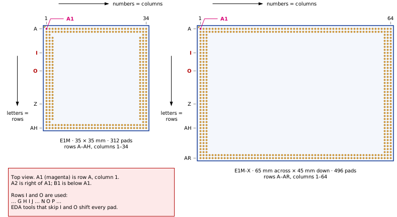
Pad coordinate frames of E1M and E1M-X (top view, pads from the pinout JSON, same scale)
1.5.2 Independent Coordinate Spaces
Each form factor has its own coordinate space: pad A1 on E1M is not the same physical position as pad A1 on E1M-X (E1M-STD §4.3). The same pad ID often carries a different signal on the other form factor, including power pads. The table below lists the pairs where a mix-up damages a module or a carrier part.
| Pad ID | On E1M | On E1M-X | Consequence of a mix-up |
|---|---|---|---|
R1, R2 | VDD (5 V input) | USB1_30_TX0_N, USB1_30_ID | 5 V on USB pads of an E1M-X module |
S1, S2 | VDD (5 V input) | GND | 5 V shorted to GND |
P1, P2 | VIO_OUT | GND | Module VIO_OUT (1.8 V) shorted to GND |
W2 | IO2 | VIO_OUT | GPIO circuit (driver, pull, load) on the module 1.8 V rail |
T1, T2, U1, U2, V1, V2 | GND, GND, BOOT2, BOOT1, BOOT3, BOOT0 | VDD_5V_IN (5 V input) | 5 V on 1.8 V boot-strap pads of an E1M module; 5 V shorted to GND |
W1 | PORn | VIO_OUT | VIO_OUT loaded by reset circuitry, or a reset button shorts the 1.8 V rail |
Z1 | JTAG_nRST | PORn | Debug reset wired to the module power-on reset |
AA1, AB1 | PDM_C0, PDM_C1 | MODULE_EN, MODULE_STBY | 5 V-tolerant control circuit on 1.8 V PDM pads |
O1, O2 | MODULE_EN, MODULE_STBY | USB1_30_RX0_N, IO3 | Control-pin circuits on USB and GPIO pads |
A19 | CAN_STBY | DAC0 | Transceiver standby on an analogue output |
AH1 | ANT_2.4GHZ | I2C0_SCL | RF feed on an I2C line |
AF1, AD1 | ANT_5GHZ, ANT_6GHZ | SPI0_CS1, SPI0_MISO | RF network on SPI pads |
F2 | UART0_TX | USB2_20_VBUS | 5 V VBUS on a 1.8 V UART pad |
I2 | USB2_VBUS | USB2_20_P | 5 V VBUS on a USB 2.0 data pad |
Q2 | GND | USB1_30_VBUS | 5 V VBUS shorted to GND |
Beyond the table, 32 more pad IDs are GND on one form factor and a signal pad on the other (for example A13, B18, D1, M1, Z2). A mixed library shorts those signals to GND. Every power, VBUS and GND pad of both pinout JSON files has been checked against the other form factor; the rows above are all the pairs where a supply pad meets a signal pad or GND.
1.5.3 Pin Names, Directions and Notation
- Pin names are the silkscreen names of the specification (E1M-STD §7.3). Where the two form factors use different silkscreen text, both names are given. The second table below lists the differences a carrier library must handle.
- A pad is written with its pad IDs, E1M first:
VDD_5V_IN(R1,R2,S1,S2/T1–V2). A single ID means the pad exists on one form factor only, which the text then names. - Signal directions are given from the module's side:
TXandSDOare module outputs,RXandSDIare module inputs. The specification states this explicitly forDBG_TX/DBG_RX(E1M-STD §7.3.10); the guide applies it to every pad. - Values are given with their units and tolerances exactly as in the source document. Dimensions in mechanical figures are in millimetres.
| E1M silkscreen | E1M-X silkscreen | Function |
|---|---|---|
VDD | VDD_5V_IN | 5 V input |
ANT_2.4GHZ, ANT_5GHZ, ANT_6GHZ | ANT_2.4GHz, ANT_5GHz, ANT_6GHz | antenna feeds |
USB0_VBUS | USB0_30_VBUS | USB0 VBUS |
USB2_P, USB2_N, USB2_ID, USB2_VBUS | USB2_20_P, USB2_20_N, USB2_20_ID, USB2_20_VBUS | USB 2.0 port |
SD_VDD (AH10) | SD_VDD_OUT (AQ30) | SD card supply output |
Module documents sometimes use their own net names, for example VDDIN for VDD_5V_IN in DS-AEN-001. This guide uses the specification names.
1.5.4 Rules for Libraries and Names
| ID | Rule | Strength | Source |
|---|---|---|---|
| CB-GEN-01 | Identify every pad by form factor and coordinate (E1M or E1M-X plus pad ID). Never refer to a pad by ID alone in a schematic, netlist or document that covers both form factors. Damage case: a pad ID read in the wrong coordinate space puts 5 V or VBUS on signal pads or shorts a supply to GND ("Same pad ID, different signal"). | MUST | E1M-STD §4.3, §7.1; damage |
| CB-GEN-02 | Generate the carrier footprint and schematic symbol from the specification pinout (pinout/v1.json for E1M, pinout/x-v1.json for E1M-X), not from a module datasheet pin table. The footprint has 312 (E1M) or 496 (E1M-X) pads and includes rows I and O. Take each pad name from the silkscreen field. Damage case: a library that skips I and O shifts every pad after row H and moves the 5 V pads onto signal pads. | MUST | E1M-STD §7.1, §9.2 (1), Annex B; damage |
| CB-GEN-03 | Do not reuse a footprint, symbol or net list of one form factor on the other (see "Same pad ID, different signal" above). | MUST NOT | E1M-STD §4.3 |
| CB-GEN-04 | Name carrier nets after the specification pin names; record module-specific names (VDDIN, SD_VDD) as aliases only. | SHOULD | Guide (informative) |
| CB-GEN-05 | When two documents disagree, apply the precedence of this chapter and the stricter value, and report the conflict to Alp Lab. | SHOULD | Guide (informative) |
1.6 How to Read a Per-Module Differences Table
Each chapter has one table titled "Per-module differences" with the columns E1M-AEN, E1M-X V2N and E1M-X V2N-M1. It explains where the modules differ and why a rule has the value it has. The rule itself is always written for the strictest column, so a carrier that follows the rule works with all three. "TBD" means the module documentation does not give the value yet; "not routed" means the module leaves the pad unconnected although the specification defines it. A per-module value is never a design target for a carrier that hosts any module.
1.7 Related Documents
| Document | Title |
|---|---|
| E1M-STD-1.0 revision 1.4 | E1M Specification (Edge-1 AI Module), with pinout/v1.json, pinout/x-v1.json and pinout/schema/loom-v1.schema.json |
| DS-AEN-001 | E1M-AEN datasheet |
| HG-AEN-001 | E1M-AEN hardware design guide |
| DS-V2N-001 | E1M-X V2N datasheet |
| HG-V2N-001 | E1M-X V2N hardware design guide |
| DS-V2N-M1-001 | E1M-X V2N-M1 datasheet |
| HG-V2N-M1-001 | E1M-X V2N-M1 hardware design guide |
| UG-E1M-001 | E1M-EVK user guide |
| UG-E1M-X-001 | E1M-X EVK user guide |
| AN-001 to AN-010 | Application notes: I2C sensors (AN-001), Wi-Fi provisioning (AN-002), MIPI CSI-2 camera (AN-003), MIPI DSI display and backlight (AN-004), CAN bus (AN-005), OTA updates (AN-006), multi-processor mailbox (AN-007), AI inference on Ethos-U and DRP-AI3 (AN-008), DeepX DX-M1 first inference (AN-009), secure boot (AN-010) |
| IPC-7351 | Generic requirements for surface-mount design and land-pattern standard |
| IPC/JEDEC J-STD-020, J-STD-033 | Moisture/reflow sensitivity classification; handling, packing and use of moisture-sensitive devices |
1.8 Chapter Checklist
| Check | Item | Rule |
|---|---|---|
| ☐ | Form factor chosen and written on the schematic title block (E1M or E1M-X). | CB-GEN-01 |
| ☐ | Footprint and symbol generated from the pinout JSON; pad count 312 or 496; rows I and O present. | CB-GEN-02 |
| ☐ | No E1M library part used on an E1M-X design, or the reverse. | CB-GEN-03 |
| ☐ | Net names follow the specification pin names. | CB-GEN-04 |
| ☐ | Document revisions used for the design recorded (specification, module datasheets). | CB-GEN-05 |
2 Designing for Any Module
A carrier that hosts any conformant module cannot rely on one module's pad use, levels or options. This chapter sets the rules that make a carrier portable across modules of the same form factor. The later chapters apply them to each interface.
2.1 The Portability Contract
The specification fixes what a module puts on a pad, but not whether it uses the pad:
- A module routes the default function of every pad it exposes, and it MAY leave any pad unconnected (E1M-STD §8.1).
- Until the specification partitions pads into mandatory and optional classes, a module MAY omit any pad that is not a power, reserved or debug pad (E1M-STD §9.3).
- Every module declares, in its per-SoM manifest, the pads it routes, the pads it does not route, the values the specification leaves to the module, and its assembly options (E1M-STD §9.1 (6), Annex C).
So a carrier sees three kinds of pad: a pad the module drives, a pad the module leaves floating, and a pad whose meaning depends on a declared module option. The carrier has to be safe in all three cases.
| ID | Rule | Strength | Source |
|---|---|---|---|
| CB-ANY-01 | The carrier stays safe, and keeps every other interface working, when any non-power, non-reserved, non-debug pad is unconnected on the module. | MUST | E1M-STD §8.1, §9.3 |
| CB-ANY-02 | Every carrier input, enable or reset that is driven from a module pad has a resistor that holds it in its safe state while the pad floats or is high-impedance. Use a pull-down where low is safe; a pull-up goes only to VIO_OUT or a rail switched by VIO_OUT. | MUST | E1M-STD §8.1, §6.2.3 (4) |
| CB-ANY-03 | Design every electrical, timing and layout value to the strictest value across the modules the carrier supports. A wider window is allowed only in a build variant that declares a SoM set whose manifests all declare that window. | MUST | E1M-STD §6.1.1 (last paragraph), §9.2 (2) |
| CB-ANY-04 | Use a pad as GPIO only in a way that stays hardware-compatible with a module that routes only the default function on that pad. | MUST | E1M-STD §8.2 |
| CB-ANY-05 | Do not depend on a tertiary (silicon-specific) function unless the build system declares the per-SoM dependency and rejects any module whose manifest does not expose it. | MUST NOT | E1M-STD §8.4, §9.2 (2) |
2.2 The Strictest-Value Rule
Where the modules differ, the carrier design value is the tightest one. The table works through the values that matter most; the chapters named in the last column give the full rule.
| Parameter | E1M-AEN | E1M-X V2N / V2N-M1 | Design value, any module | Source |
|---|---|---|---|---|
VDD_5V_IN at the pads | 4.75 / 5.0 / 5.25 V | 4.5 / 5.0 / 5.5 V | 4.75– 5.25 V | §6.1.1 (1), ch. 5 |
VDD_5V_IN absolute maximum | 5.5 V | 6.0 V | ≤ 5.5 V, including transients | §6.1.1 (2), ch. 5 |
VDD_5V_IN ramp 0 V to 4.75 V | monotonic, ≤ 40 ms | not specified | monotonic, ≤ 40 ms | §6.1.1 (3), ch. 5 |
| Carrier bulk capacitance at the pads | ≥ 50 μF effective per A of total load | ≥ 10 μF + 100 nF | the larger of the two | §6.1.1 (7), ch. 5 |
VIO_OUT level | 1.8 V (tolerance TBD) | 1.8 V ± 5 % | 1.8 V ± 5 % | §6.1.2 (1), ch. 6 |
VIO_OUT carrier load | ≤ 100 mA; ≤ 50 mA in the first 2 ms; ≤ 2.5 μF | TBD | ≤ 100 mA; ≤ 50 mA in the first 2 ms; ≤ 2.5 μF | §6.1.2 (4), ch. 6 |
| 1.8 V pad absolute maximum | − 0.3 V to 1.98 V | − 0.3 V to 1.98 V | − 0.3 V to 1.98 V | §6.2.3 (5), ch. 7 |
Carrier outputs after PORn falls | Hi-Z or low within 1 ms | TBD | Hi-Z or low within 1 ms | §6.2.2 (2), ch. 8 |
PORn carrier low pulse | ≥ 2 ms | TBD | ≥ 2 ms | §6.3.1 (3), ch. 8 |
| USB 2.0 intra-pair skew | ≤ ± 5 ps | ± 2 ps | ± 2 ps | HG-AEN-001, HG-V2N-001, ch. 4 |
| Ambient operating temperature | − 40 to +75 °C | − 40 to +85 °C | − 40 to +75 °C | DS-AEN-001, DS-V2N-001 |
2.3 I/O Voltage Domains
VIO_OUT is 1.8 V in this revision of the specification, and every reference module is a 1.8 V module (E1M-STD §6.1.2 (1)). Every signal pad is in the VIO_OUT domain unless the specification or the module manifest names another domain (E1M-STD §6.7.1). Figure 3 shows the domains a typical carrier has and where they meet.
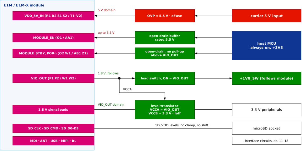
Carrier voltage domains around a module
The pads below are not 1.8 V VIO_OUT-domain pads. A carrier does not clamp them to VIO_OUT, pull them up to VIO_OUT or level-translate them as 1.8 V signals.
| Pads | Domain | Carrier rule |
|---|---|---|
MODULE_EN | up to 5.5 V | Open-drain to GND; parts rated 5.5 V (E1M-STD §6.3.1 (1), Chapter 8). |
VDD_5V_IN / VDD | 5 V input | E1M-STD §6.1.1, Chapter 5. |
VIO_OUT, SD_VDD_OUT / SD_VDD, +V_CAM0–+V_CAM3 | module supply outputs | Never drive, back-feed or connect another supply (E1M-STD §6.7.1). |
SD_CLK, SD_CMD, SD_D0–SD_D3 | SD_VDD_OUT / SD_VDD | Drive or pull up only to the card-supply level and only while it is on. E1M-AEN: 3.4 V card side; E1M-X V2N / V2N-M1: 1.8 V / 3.3 V, switched automatically. |
BL_LED_A, BL_LED_K | backlight LED string | LED string and feedback network only. E1M-AEN BL_LED_A reaches up to 36 V. |
ETH0_*, ETH1_* MDI pairs | PHY MDI | Magnetics and ESD only (E1M-STD §7.3.6, Chapter 11). |
ANT_* | RF | 50 Ω feed (E1M-STD §7.3.2, Chapter 12). |
USB* data, USB*_VBUS, USB_CC1, USB_CC2 | USB | Per the USB specifications (Chapter 13). |
CSI*, DSI*, PCIE* | high-speed differential | Per the MIPI and PCIe specifications. |
CANxH/CANx_TX, CANxL/CANx_RX | bus level or VIO_OUT, per the declared CAN option | E1M-STD §6.7.2, §7.3.14, Chapter 18. |
+S_CAP | RTC backup store | As the module manifest declares (Chapter 10). |
Two pads tolerate more than 1.8 V on one module only. A carrier that hosts any module treats them as 1.8 V VIO_OUT-domain pads:
MODULE_STBY(O2/AB1): 5 V tolerant on E1M-AEN R3; pulled up to the module 1.8 V rail on E1M-X V2N. The specification states that it is not 5 V tolerant on every module (E1M-STD §6.3).- E1M pad
P3(IO25):RTC_WAKE_N, an open-drain wake output, on E1M-AEN R3; a 1.8 V GPIO on other modules, absolute maximum 1.98 V. On E1M-X,IO25is padF63. It leaves theVIO_OUTdomain only for a module whose manifest declares it in another domain (E1M-STD §6.7.1).
PORn (W1 / Z1) is not 5 V tolerant on any module: it is pulled up to 1.8 V on every module, and the carrier only pulls it low with an open-drain output and never drives it high (E1M-STD §6.3.1 (3)).
2.3.1 3.3 V Peripherals on a 1.8 V Module
A 3.3 V peripheral connects through a level translator whose module-side supply (VCCA) is VIO_OUT and whose peripheral side (VCCB) is the carrier 3.3 V rail. Open-drain buses (I2C) use an open-drain translator with pull-ups on each side, the module side to VIO_OUT.
| ID | Rule | Strength | Source |
|---|---|---|---|
| CB-ANY-06 | Treat every signal pad not listed in the table above, or declared otherwise in the module manifest, as a 1.8 V VIO_OUT-domain pad: keep it between − 0.3 V and 1.98 V at all times. | MUST | E1M-STD §6.2.3 (5), §6.7.1 |
| CB-ANY-07 | Do not clamp, pull up to VIO_OUT or level-translate as 1.8 V signals the pads listed in the table above. | MUST NOT | E1M-STD §6.7.1 |
| CB-ANY-08 | Every level translator referenced to VIO_OUT keeps both ports high-impedance while VIO_OUT is off (Ioff or partial-power-down specified). Some pass-gate translators conduct with VCCA at 0 V and do not qualify. | MUST | E1M-STD §6.1.2 (5) |
| CB-ANY-09 | Choose translators whose VCCA is rated 1.65– 3.6 V, so the carrier part still fits if a later revision of the specification defines another VIO_OUT level. Design for 1.8 V today. | SHOULD | E1M-STD §6.1.2, note (informative) |
The specification defines no 3.3 V VIO_OUT class. The 1.65– 3.6 V VCCA recommendation is forward compatibility only; a carrier never assumes a 3.3 V module.
2.4 Interfaces a Module May Not Route
The reference modules route different subsets of the pinout. Figure 4 compares them with the specification.
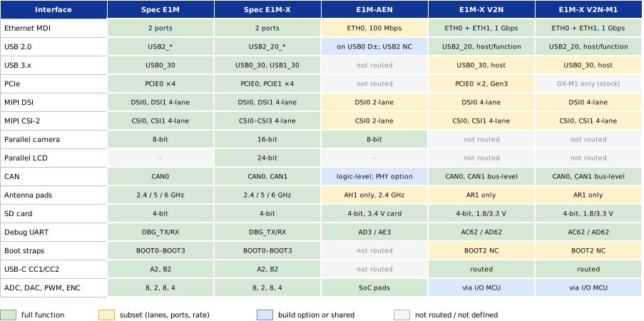
Interfaces defined by the specification and routed by the reference modules
For each interface, the carrier has to behave sensibly when the module does not route it:
| Interface | What a module may do | Carrier behaviour |
|---|---|---|
| Ethernet | Route one port only, or only pairs DA and DB (100BASE-TX). | Route all four pairs of every port the carrier uses, with 1000BASE-T magnetics (E1M-STD §7.3.6 (3)). A port without a PHY has no link and no other effect. |
| USB 3.x | Route no SuperSpeed lanes (E1M-AEN), or USB0 only (E1M-X V2N / V2N-M1). | The connector still works at USB 2.0 when its D± pair is wired to the routed USB 2.0 group (see the assembly-variant table). |
| PCIe | Route nothing (E1M-AEN) or lanes 0– 1 of PCIE0 (E1M-X V2N). On E1M-X V2N-M1 the stock boot firmware routes PCIE0 to the on-module DX-M1 on every boot and has no API to switch it, so a carrier device on PCIE0_* is not reachable with the stock image (HG-V2N-M1-001). | Hold the slot device in reset (pull-down on its reset) and keep slot power off by default; enable slot power from a module GPIO with a pull-down (CB-ANY-10, Chapter 17). A carrier PCIe slot does not work with E1M-X V2N-M1 (CB-ANY-11). |
| MIPI DSI, CSI-2 | E1M-AEN: DSI0 and CSI0, 2 lanes. E1M-X V2N / V2N-M1: DSI0 4 lanes, CSI0 and CSI1 4 lanes each. DSI1, CSI2 and CSI3 are not routed. | Select panels and sensors that run on the smallest lane count of the supported SoM set (CB-ANY-11). |
| Parallel camera, LCD | Not routed on E1M-X V2N / V2N-M1. | A parallel sensor or panel works only with modules that route the interface; declare the SoM set. |
| Antenna | Drive the 2.4 GHz pad only and declare the 5 GHz and 6 GHz pads unused (E1M-AEN AH1; E1M-X V2N AR1, E1M-STD §6.5). | Default fit uses the 2.4 GHz pad only (CB-ANY-16). |
| Boot straps | Ignore the strap and declare it, with the pads not connected (E1M-AEN, E1M-STD §6.4 (3)); BOOT2 not connected (E1M-X V2N). | Keep the strap circuit for every module; it has no effect on a floating pad (Chapter 9). |
USB_CC1, USB_CC2 | Not routed (E1M-AEN). | Carrier Rd fit or not-fit options (Chapter 13). |
| ADC, DAC, PWM, encoder | Served by an on-module I/O MCU (E1M-X V2N / V2N-M1). | Same pads and levels; timing and latency differ by module. |
| ID | Rule | Strength | Source |
|---|---|---|---|
| CB-ANY-10 | A carrier device on an interface that a supported module may not route stays unpowered or in reset while its module-side pads float (slot power off, reset held low by a resistor). | SHOULD | E1M-STD §8.1; Guide (informative) |
| CB-ANY-11 | Choose display panels and camera sensors that work with the smallest lane count and link rate of the supported SoM set (E1M-AEN: two-lane DSI and CSI-2, 100 Mbps Ethernet, USB 2.0 only), or declare the SoM set that the part needs. A carrier PCIe device on PCIE0_* that the product needs restricts the SoM set: E1M-X V2N-M1 does not reach it with the stock image. | SHOULD | E1M-STD §9.2 (2); DS-AEN-001, DS-V2N-001, HG-V2N-M1-001 |
2.5 Dual-Meaning Pads and Assembly Variants
Some pad groups carry different signals depending on the module or its assembly option. A carrier that supports more than one meaning uses assembly options: 0 Ω links that are fitted or not fitted (DNP), BOM variants, or a switch. The specification sets three requirements for every such group (E1M-STD §6.7.2):
- The default assembly (the fit used when no SoM set is declared) is the fit that cannot damage any conformant module.
- Two paths of the same group are never both fitted.
- Every carrier build variant declares the fit of each group and the modules it supports.
Figure 5 shows the pattern with the CAN pads, the group the specification itself defines.
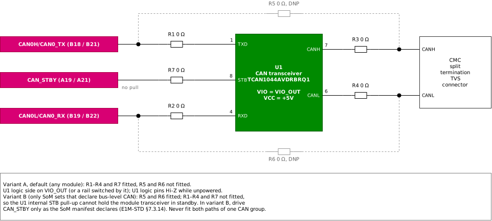
Assembly-option pattern for a dual-meaning pad group (CAN)
A CAN bus connected straight to the CAN pads destroys the SoC of a module that uses logic-level CAN, such as the E1M-AEN standard build.
| Pad group | Mechanism | Safe default fit | Other fit (declared SoM set only) |
|---|---|---|---|
CAN0H/CAN0_TX, CAN0L/CAN0_RX (B18, B19 / B21, B22); CAN1 (B24, B25, E1M-X) | 0 Ω links | Carrier transceiver connected to the pads; bypass links not fitted. | Bypass fitted, transceiver links not fitted: only if every module of the SoM set declares bus-level CAN for that group. |
CAN_STBY (A19 / A21) | 0 Ω link | No carrier pull; connected through a 0 Ω link only to the carrier transceiver standby input. | Link not fitted, so the internal standby pull of the carrier transceiver cannot hold an on-module transceiver in standby. The carrier drives CAN_STBY only if the SoM manifest declares it a SoM input, with the declared polarity (E1M-STD §7.3.14). |
USB 2.0 D±: USB0_30_D_P/N (B1, C1 / B1, C1) and USB2_P/N (I1, J1) / USB2_20_P/N (I2, J2) | 0 Ω links or a USB 2.0 switch | Connector on USB0_30_D_P/N; USB2 links not fitted. | Connector on the USB2 group (E1M-AEN R2, or a second USB 2.0 port of E1M-X V2N). |
BL_LED_A / BL_PWM (A31 / B55), BL_LED_K (B31 / A55) | 0 Ω links | LED string anode on BL_LED_A, cathode through RFB to GND on BL_LED_K; any link to a carrier backlight driver input not fitted. | Carrier driver on BL_PWM, for modules built without the on-module driver; LED string not connected. |
ANT_2.4GHz, ANT_5GHz, ANT_6GHz (AH1, AF1, AD1 / AR1, AP1, AN1) | 0 Ω links | Only the 2.4 GHz pad linked to the antenna path. | 5 GHz and 6 GHz pads linked when every module of the SoM set drives them. |
E1M P3 (IO25, RTC_WAKE_N on E1M-AEN) | pull-up fit | No pull-up, or a pull-up to VIO_OUT only. | Pull-up to an always-on rail ≤ 5.5 V: only if every module of the declared SoM set lists P3 in its manifest as a pad outside the VIO_OUT domain (E1M-STD §6.7.1). |
+S_CAP (AG15 / AQ25) | store fit | Chapter 10. | Chapter 10. |
| ID | Rule | Strength | Source |
|---|---|---|---|
| CB-ANY-12 | For every dual-meaning pad group, make the default assembly the fit that cannot damage any conformant module; never fit two paths of the same group; declare the fit and the supported modules of every build variant. | MUST | E1M-STD §6.7.2 (1), (4), (5), §9.2 (8) |
| CB-ANY-13 | CAN: default assembly is the carrier-transceiver path with the bypass not fitted; the bypass is fitted only in a variant whose SoM set is bus-level CAN throughout. The carrier transceiver takes its logic-side supply from VIO_OUT or a carrier rail switched by VIO_OUT, and its logic pins are high-impedance while it is unpowered. CAN_STBY reaches the transceiver standby input through a 0 Ω link that is not fitted in the bypass variant; there the carrier drives CAN_STBY only as the SoM manifest declares. | MUST | E1M-STD §6.7.2 (2), (3), §7.3.14 |
| CB-ANY-14 | USB 2.0: do not fit links from both USB0_30_D_P/N and the USB2 group to one connector. On E1M-X V2N both groups are live PHYs. | SHOULD NOT | DS-V2N-001 Digital Pins; Guide |
| CB-ANY-15 | Backlight: the default fit connects only an LED string to BL_LED_A; a path from BL_LED_A / BL_PWM to a logic or driver input is not fitted by default. Make the carrier RFB a part that can be left unfitted. | MUST | E1M-STD §6.7.1, §6.7.2 (1) |
| CB-ANY-16 | Antenna: leave the pads a module does not drive unconnected; by default only the 2.4 GHz pad is linked to the antenna path. | MUST | E1M-STD §7.3.2 |
| CB-ANY-17 | Do not pull E1M pad P3 up to any rail other than VIO_OUT (or a rail switched by VIO_OUT), except in a variant whose declared SoM set consists only of modules whose manifests list P3 as a pad outside the VIO_OUT domain. | MUST NOT | E1M-STD §6.2.3 (4), (5), §6.7.1 |
The E1M-EVK (UG-E1M-001, board 2641-R3) uses these defaults. They are a worked example, not additional rules:
| Group | Fitted (default) | Not fitted |
|---|---|---|
| CAN | U6 TCAN1044AVDRBRQ1; R34, R246 (logic side) and R247, R248 (bus side), 0 Ω | R249, R250 0 Ω bypass |
Antenna (AH1) | R132 0 Ω to the chip antenna | R111 0 Ω to the U.FL connector |
| Backlight | BL_LED_A, BL_LED_K to the panel connector; R9 2.4 Ω from BL_LED_K to 0 V | R109 (BL_LED_A to BL_PWM) |
| RTC backup | store selected on header P16 | R223 0 Ω from +S_CAP to 0 V |
2.6 Pads a Generic Carrier Must Not Use
Three groups of pads are off limits to a carrier that targets any module.
Reserved pads. RSVD pads can carry live module nets used in production. The specification lists 34 on E1M and 20 on E1M-X (E1M-STD §7.3.3). The known uses on the reference modules show the damage a connection can do:
| Pads | Module use | Effect of a carrier connection |
|---|---|---|
E1M W3 | E1M-AEN 1.8 V rail (identity EEPROM supply) | Back-feeds or loads the module 1.8 V domain |
E1M U3, V3 | E1M-AEN 3.3 V programming port / private I2C, 4.7 kΩ pull-ups to 3.3 V | 3.3 V on a 1.8 V carrier bus; corrupts the power controller and RTC |
E1M S3 | E1M-AEN Wi-Fi module reset (open drain) | Holds the radio in reset |
E1M Q3, R3, T3 | E1M-AEN Wi-Fi module debug: SWDIO, SWCLK, log UART TX (1.8 V, only while Wi-Fi is powered) | Back-powers the radio; contention |
E1M-X W62–AB62, AE62–AR62 | E1M-X V2N / V2N-M1 production use | Not documented; treat as live |
Pads a module does not route. A pad that one module leaves unconnected keeps its standard function on other modules. The permission to route through a pad applies only to pads whose default function in the specification is NC (E1M-STD §7.3.4; E1M-X only, see Chapter 4).
Pads owned by on-module devices. Some default-function pads are wired to an on-module coprocessor instead of the SoC, or sit on an internally switched rail:
| Module and pads | Owner and behaviour | Carrier rule |
|---|---|---|
E1M-AEN IO13, IO15–IO24 (E3, F3–O3); SPI1 (AG8, AG9, AG10, AH8, AH9) | Wi-Fi / BLE module (CC3501E) pads, powered only while Wi-Fi is on, also while the SoC runs | Never drive them while the Wi-Fi supply is off. Pull-downs only: no pull-up to VIO_OUT or any other rail, because VIO_OUT stays high while the Wi-Fi rail is off and a pull-up then back-powers the CC3501E (E1M-STD §6.2.3 (1), (7)). |
E1M-X V2N / V2N-M1 IO8–IO16, IO25–IO32, IO34, IO35, I2C3, PWM0–PWM7, ENC0–ENC3, ADC, DAC | On-module GD32 I/O MCU, reached through Alp Lab bridge firmware | Usable; latency and power-state behaviour differ from SoC pads. IO33 (AQ63) is not routed. |
E1M-X V2N-M1 IO0–IO6 (L2, M2, N2, O2, AF2, AG2, AL2), IO17–IO22 (AQ26, AR26, AQ27, AR27, AQ28, AR28), IO24 (AR29) | Routed to the on-module DX-M1; usable as carrier GPIO only after a DeepX software patch (DS-V2N-M1-001) | Keep them carrier inputs or unconnected by default; never drive them in a variant that supports E1M-X V2N-M1 (CB-ANY-20). |
DS-AEN-001 allows a pull-up of ≥ 100 kΩ to VIO_OUT on the E1M-AEN Wi-Fi pads. E1M-STD §6.2.3 (1) and (7) forbid any pull-up into a switched pad group while its rail is off, and the specification takes precedence. The conflict is listed in Annex C.
| ID | Rule | Strength | Source |
|---|---|---|---|
| CB-ANY-18 | Leave every RSVD pad unconnected: no trace, test point, pull resistor, load or jumper. | MUST | E1M-STD §7.3.3, §9.2 (9) |
| CB-ANY-19 | Do not route an unrelated net through a pad that any supported module does not route (described as "NC" in a module datasheet or listed in the manifest not_routed). | MUST NOT | E1M-STD §7.3.4, §9.2 (9) |
| CB-ANY-20 | Do not drive, or pull up, a pad that a supported module wires to an on-module device or to an internally switched rail while that device or rail can be off or driving: E1M-AEN Wi-Fi pads and SPI1, plus IO8–IO11 (AG33, AH34, AH33, A18) on a carrier that declares E1M-AEN R2 support; E1M-X V2N-M1 DX-M1 pads. Pull-downs are permitted. | MUST NOT | E1M-STD §6.2.3 (1), (7); DS-AEN-001 Digital Pins, Hardware Revisions; DS-V2N-M1-001 Digital Pins |
2.7 Module Hardware Revisions
A module's hardware revision is held in its identity EEPROM, not in the MPN (DS-V2N-001 MPN Decoder). For E1M-AEN, revision R2 differs from R3 in ways a carrier can see:
| Item | R2 | R3 | Carrier consequence |
|---|---|---|---|
SD_VDD (AH10) | supply input from the carrier | 3.4 V output, switched by firmware | A carrier supply on AH10 fights an R3 module. Never connect a supply to it (E1M-STD §6.7.1). |
| Reset supervisor | none (erratum E-02, Alif ER004) | on-module supervisor | R2 on E4, E6, E8: the SoC must be held in reset below 1.65 V or it can be permanently damaged. See the E1M-AEN errata. |
| USB 2.0 pads | I1, J1, I2, J2 | B1, C1, C2, D2 | Option links on both groups (assembly-variant table). |
CSI-2 polarity (P33/P34, Q33/Q34, R33/R34) | P and N swapped on the module | as listed in DS-AEN-001 | Polarity swap in the sensor or a carrier variant. |
VIO_OUT | 200 mA | 100 mA, ≤ 2.5 μF | Design to the R3 limit. |
| 5 V window | 4.5– 5.5 V | 4.75– 5.25 V | Design to the R3 window. |
MODULE_STBY (O2) | 1.8 V RTC event input, 100 kΩ pull-up to 1.8 V | 5 V tolerant control input | No pull-up above VIO_OUT (Chapter 8). |
IO8–IO11 (AG33, AH34, AH33, A18) | Wi-Fi module GPIOs | SoC GPIOs | On R2, driving or pulling them up while Wi-Fi is off back-powers the radio (CB-ANY-20). |
IO21–IO24 (L3, M3, N3, O3) | not connected | Wi-Fi module GPIOs | Treat as Wi-Fi-owned pads (CB-ANY-20). |
IO25 (P3) | not connected | RTC_WAKE_N, open-drain wake output | CB-ANY-17. |
+V_CAM0, +V_CAM1 (Z34, AB34) | 0.6– 3.3 V, 300 mA each | 0.6– 3.1 V, 170 mA combined | Size camera loads to the R3 values (Chapter 15). |
MODULE_EN (O1) | module enable, no glitch filter | module enable with a 1.0 ms glitch filter, 5 V tolerant | Do not rely on the filter; keep MODULE_EN free of glitches (Chapter 8). |
+S_CAP (AG15) | — (not used) | RTC backup input: carrier store, or tie to GND | Chapter 10. |
| ID | Rule | Strength | Source |
|---|---|---|---|
| CB-ANY-21 | A carrier that may receive an E1M-AEN R2 module declares it, follows DS-AEN-001 "Hardware Revisions" and the E1M-AEN errata, and never connects a supply to AH10. | MUST | E1M-STD §6.7.1; DS-AEN-001 Hardware Revisions |
2.8 Identifying the Module at Run Time
A carrier that supports more than one module tells them apart at run time and checks that the fitted module is in its declared SoM set:
- Per-SoM manifest. The manifest declares the routed pads, tertiary functions, CAN option, 5 V and
VIO_OUTvalues and switched pad groups (E1M-STD Annex C). The carrier build system reads it and rejects a module it does not support (E1M-STD §8.4). - Identity EEPROM. E1M-AEN carries a 128 Kbit identity EEPROM on
I2C0(AD2/AE2on E1M) at 7-bit addresses0x50(array) and0x58(identity page), powered from the module 1.8 V rail, so it answers only whileVIO_OUTis high (DS-AEN-001 "Identity EEPROM and I2C0"). DS-V2N-001 calls the E1M-X V2N EEPROM onI2C0optional and does not state its address; the hardware revision is held in the on-module identity EEPROM (DS-V2N-001 MPN Decoder). - On-module I2C devices on E1M-X. The E1M-X V2N / V2N-M1 power management is on I2C: main PMIC
ACT88760at0x25/0x26and secondary PMICDA9292at0x1E(E1M-STD Annex A, V2N and V2N-M1 families). The bus they sit on is not stated. The modules also carry a TPM and a TMP112D-class temperature sensor; their addresses are not stated. On E1M-X V2N-M1, a second writer to the PMIC can bring the 0.75 V DX-M1 core rail up at the PMIC's 1.80 V default, which can damage the DX-M1 (HG-V2N-M1-001). - Firmware. The Alp SDK reads the identity EEPROM and selects the module support package.
| ID | Rule | Strength | Source |
|---|---|---|---|
| CB-ANY-22 | Read the module identity (identity EEPROM or manifest) before enabling an interface that only part of the supported SoM set provides, and keep that interface off for any other module. Do not place a carrier device at 0x50 or 0x58 on I2C0 (Chapter 19). | SHOULD | E1M-STD §8.4, Annex C; DS-AEN-001 |
| CB-ANY-23 | On a carrier that supports E1M-X, place no carrier device at 0x1E, 0x25, 0x26, 0x50 or 0x58 on any module I2C bus (I2C0–I2C3), and add no second I2C master on those buses, until Alp Lab states which buses carry the on-module PMICs, EEPROM, TPM and temperature sensor. Reserve the TPM and temperature-sensor addresses as well once they are published. | MUST NOT | E1M-STD Annex A; HG-V2N-M1-001 (DX-M1 damage) |
2.9 Per-Module Differences
| Item | E1M-AEN | E1M-X V2N | E1M-X V2N-M1 |
|---|---|---|---|
| CAN | Standard build: no transceiver, B18 / B19 1.8 V logic, A19 SoC GPIO (logic-level CAN). Option: TCAN1044AVDRBRQ1 on-module, bus-level. | Two on-module CAN PHYs, bus-level (DS-V2N-001 calls them optional) | as E1M-X V2N |
| Backlight | On-module KTD2801ECD-TR boost driver; variant without driver: A31 = BL_PWM | On-module driver, optional; B55 = BL_LED_A / BL_PWM | as E1M-X V2N |
| Antenna | Feed on AH1 (2.4 GHz only); on-module I-PEX MHF 4L connector is an assembly option (not fitted as standard) | AR1 "ANT_2.4GHz / NC"; AP1, AN1 not connected; on-module U.FL option | as E1M-X V2N |
| USB 2.0 D± | B1 / C1 (R3); I1 / J1 not connected | B1 / C1 (USB0, USB 3.2 host) and I2 / J2 (USB2, host or function), both live | as E1M-X V2N |
| Pads owned by on-module devices | Wi-Fi: IO13, IO15–IO24, SPI1 | GD32 I/O MCU: IO8–IO16, IO25–IO32, IO34, IO35, I2C3, PWM, ENC, ADC, DAC | as E1M-X V2N, plus DX-M1: IO0–IO6, IO17–IO22, IO24 |
RSVD pads | 34; W3, U3, V3, S3, Q3, R3, T3 carry live nets | 20, production use | 20, production use |
| Identity | EEPROM at 0x50 / 0x58 on I2C0 | EEPROM on I2C0 ("optional" in DS-V2N-001), address TBD | EEPROM on I2C0, address TBD |
| On-module I2C devices to protect | identity EEPROM 0x50 / 0x58 | ACT88760 0x25 / 0x26, DA9292 0x1E; bus TBD | as E1M-X V2N; a second PMIC writer can damage the DX-M1 |
Carrier PCIe device on PCIE0_* | not routed | lanes 0– 1, Gen3 | not reachable with the stock image (lanes routed to the DX-M1 on every boot) |
2.10 Chapter Checklist
| Check | Item | Rule |
|---|---|---|
| ☐ | Supported SoM set written down for every build variant. | CB-ANY-03, CB-ANY-12 |
| ☐ | Every carrier input driven from a module pad has a default pull to its safe state. | CB-ANY-01, CB-ANY-02 |
| ☐ | Design values taken from the strictest-value table. | CB-ANY-03 |
| ☐ | Pad GPIO use compatible with default-function modules; no undeclared tertiary function. | CB-ANY-04, CB-ANY-05 |
| ☐ | Every non-VIO_OUT pad identified; none clamped or translated as 1.8 V. | CB-ANY-06, CB-ANY-07 |
| ☐ | Translators Ioff-rated, VCCA = VIO_OUT, VCCA range 1.65– 3.6 V. | CB-ANY-08, CB-ANY-09 |
| ☐ | Optional-interface devices held off or in reset by default. | CB-ANY-10 |
| ☐ | Panels and sensors run on two lanes, or the SoM set is declared. | CB-ANY-11 |
| ☐ | CAN default fit is the carrier-transceiver path; never both paths fitted; transceiver logic side on VIO_OUT, Hi-Z unpowered; CAN_STBY link not fitted in the bypass variant. | CB-ANY-13 |
| ☐ | Only one USB 2.0 group linked to each connector. | CB-ANY-14 |
| ☐ | Backlight default fit is the LED string; RFB can be left unfitted. | CB-ANY-15 |
| ☐ | Only the 2.4 GHz antenna pad linked by default. | CB-ANY-16 |
| ☐ | E1M P3 pulled up only to VIO_OUT, unless every SoM-set manifest lists P3 outside the VIO_OUT domain. | CB-ANY-17 |
| ☐ | No connection to any RSVD pad; no foreign net through a module-unrouted pad. | CB-ANY-18, CB-ANY-19 |
| ☐ | On-module-owned pads never driven or pulled up (Wi-Fi pads, R2 IO8–IO11, DX-M1 pads). | CB-ANY-20 |
| ☐ | E1M-AEN R2 support decided; no supply on AH10. | CB-ANY-21 |
| ☐ | Module identity read before optional interfaces are enabled. | CB-ANY-22 |
| ☐ | E1M-X: no carrier device at 0x1E, 0x25, 0x26, 0x50, 0x58; no second I2C master on module buses. | CB-ANY-23 |
3 Footprint, Mechanics and Assembly
A module is a connectorless land-grid-array (LGA) part that is reflow-soldered to the carrier. This chapter covers the carrier land pattern, keep-outs, the two mounting options, reflow and handling.
3.1 Outlines and Pad Bands
| Attribute | E1M | E1M-X |
|---|---|---|
| Outline | 35 × 35 mm, ± 0.1 mm (TBD) | 65 mm across × 45 mm down, ± 0.1 mm (TBD) |
| Pads | 312, LGA | 496, LGA |
| Coordinate space | rows A–AH (down), columns 1– 34 (across) | rows A–AR (down), columns 1– 64 (across) |
| Pad band (from the pinout JSON) | two pads deep along the top and bottom edges (rows A, B and AG, AH); three pads deep along the left and right edges (columns 1– 3 and 32– 34) | two pads deep along the long (top and bottom) edges (rows A, B and AQ, AR); three pads deep along the short (left and right) edges (columns 1– 3 and 62– 64) |
| Central cavity (top view) | 27.0 mm across × 29.0 mm down, R1.00 corners, 4.0 mm from the left edge, 3.0 mm from the top edge (centred) | 57.45 mm across × 39.45 mm down, R1.00 corners, 3.775 mm from the left edge, 2.775 mm from the top edge (centred) |
| Source | E1M-STD §4.1, §5.1.1 | E1M-STD §4.2, §5.1.2 |
The central cavity is the area inside the pad band. It carries no pads.
Every figure of this guide uses the pad frame of Chapter 1, which is the frame of the alplab.ai pinout viewer and of the E1M-STD pinout JSON: top view (component side up), A1 the top-left corner pad at the pin-1 fiducial, the pad letters are the rows, top to bottom, and the pad numbers are the columns, left to right. A2 is directly right of A1; B1 is directly below A1. On E1M, rows A, B and AG, AH form the bands along the top and bottom edges, two pads deep; columns 1– 3 and 32– 34 form the bands along the left and right edges, three pads deep; the cavity measures 27.0 mm across and 29.0 mm down. The E1M-X is landscape: the outline is 65 mm across (columns 1– 64) and 45 mm down (rows A–AR), and the cavity measures 57.45 mm across and 39.45 mm down. Rows A, B and AQ, AR are two pads deep; columns 1– 3 and 62– 64 are three pads deep.
3.2 Carrier Land Pattern
3.2.1 E1M
The specification fixes the E1M signal grid: pads lie on a 1.0 mm pitch grid and are 0.40 mm diameter round copper pads (E1M-STD §5.1.1). The 0.5 mm value in the footprint drawing of earlier revisions is the size of the A1 fiducial, not the pitch. E1M-STD §5.1.3 gives a recommended carrier land pattern for both form factors (informative; its values are those published for E1M-AEN), and the land pattern published for E1M-AEN completes the footprint (Figure 6). E1M-STD-1.0 revision 1.5 does not specify pad position and size tolerances or a carrier footprint library.
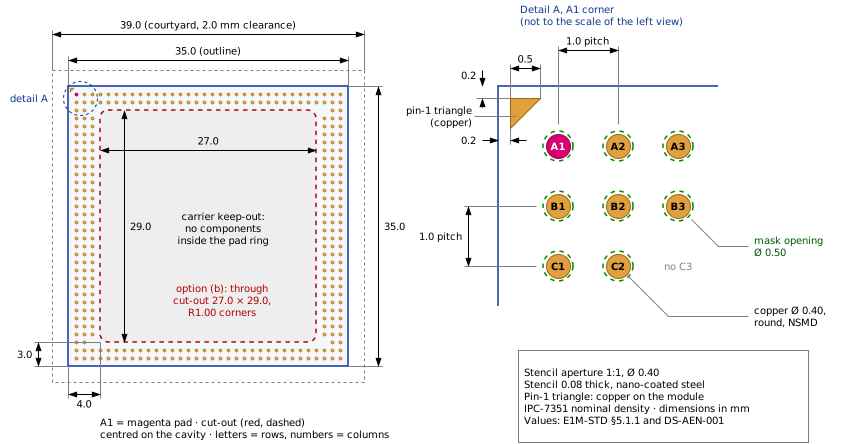
E1M carrier land pattern: top view with 2.0 mm courtyard, keep-out and the option (b) cut-out, and pad detail
| Parameter | Value | Source |
|---|---|---|
| Pad pitch (signal grid) | 1.0 mm | E1M-STD §5.1.1 (normative) |
| Copper pad | 0.40 mm diameter, round | E1M-STD §5.1.1 (normative) |
| Pad type | non-solder-mask-defined (NSMD) | E1M-STD §5.1.1, informative; DS-AEN-001 |
| Solder-mask opening | 0.50 mm diameter | E1M-STD §5.1.1, informative; DS-AEN-001 |
| Stencil aperture | 1:1, 0.40 mm diameter | E1M-STD §5.1.1, informative; DS-AEN-001 |
| Stencil | nano-coated steel, 0.08 mm thick (recommended) | DS-AEN-001 |
| Density level | IPC-7351 nominal, LGA | DS-AEN-001 |
3.2.2 E1M-X
The E1M-X land pattern is published in DS-V2N-001 0.10 and DS-V2N-M1-001 0.13 (Recommended PCB Land Pattern): 1.00 mm pad pitch (signal grid), ⌀ 0.40 mm round NSMD copper pads (one pad size for the whole pad band), ⌀ 0.50 mm solder-mask opening, 1:1 ⌀ 0.40 mm stencil aperture, 80 μm nano-coated steel stencil, and a 2.0 mm courtyard around the module outline, 69.0 × 49.0 mm. These values agree with the E1M-STD §5.1.2 footprint drawing and the §5.1.3 recommended carrier land pattern of E1M-STD-1.0 revision 1.5. In revision 1.5 they are still informative for E1M-X: the specification has no normative (SHALL) text for E1M-X pad pitch and size, no dimension callouts, no pad tolerances and no footprint library (§5.1.2, §5.1.3). The pinout JSON places 64 columns across 65 mm and 44 rows down 45 mm, which is consistent with the 1.0 mm grid. Figure 7 shows the outline, cavity, option (b) cut-out and courtyard in the pad frame of Chapter 1 (landscape, A1 top left).
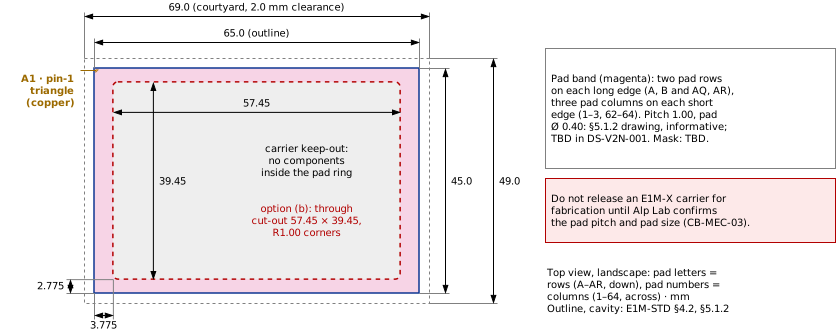
E1M-X outline, pad band, cavity, option (b) cut-out and 2.0 mm courtyard (pad dimensions per DS-V2N-001 0.10)
Build the E1M-X footprint from the land-pattern table of DS-V2N-001 0.10 / DS-V2N-M1-001 0.13 and the pad coordinates of pinout/x-v1.json (CB-MEC-01, CB-MEC-03). Do not derive it from photos. Pad position and size tolerances are not yet specified (E1M-STD-1.0 revision 1.5, §5.1.3).
| ID | Rule | Strength | Source |
|---|---|---|---|
| CB-MEC-01 | Make the mating land pattern match the chosen form factor: every pad at the coordinate of the pinout JSON, module A1 at the carrier A1 mark. | MUST | E1M-STD §9.2 (1), §7.1 |
| CB-MEC-02 | E1M: place the signal pads on a 1.0 mm pitch grid as 0.40 mm diameter round copper pads. | MUST | E1M-STD §5.1.1 |
| CB-MEC-03 | E1M-X: place the signal pads on a 1.00 mm pitch grid as ⌀ 0.40 mm round copper pads, per the module land pattern (the §5.1.2 drawing and §5.1.3 show the same values, informative). | MUST | E1M-STD §9.2 (1), §5.1.2 drawing, §5.1.3; DS-V2N-001 0.10, DS-V2N-M1-001 0.13 Recommended PCB Land Pattern |
| CB-MEC-04 | Use NSMD pads with a 0.50 mm mask opening, a 1:1 0.40 mm stencil aperture and a 0.08 mm nano-coated steel stencil (E1M). On E1M-X, use NSMD pads with a ⌀ 0.50 mm mask opening, a 1:1 ⌀ 0.40 mm stencil aperture and an 80 μm nano-coated steel stencil. | SHOULD | E1M-STD §5.1.1, §5.1.3 (informative); DS-AEN-001; DS-V2N-001 0.10, DS-V2N-M1-001 0.13 |
3.3 Keep-Outs and Placement
- Inside the pad ring. A module is never soldered flat on a solid carrier: the carrier uses one of the two mounting options below, a spacer PCB or a through cut-out under the module cavity. E1M-AEN forbids carrier components inside the pad ring; E1M-X V2N / V2N-M1 forbid components taller than a TBD height there. The rule for any module is the stricter one: no components. With option (a) this covers the carrier under the module cavity, even though the spacer raises the module: the carrier keeps the cavity area clear of components (E1M 27.0 mm across × 29.0 mm down, 4.0 mm from the left and 3.0 mm from the top outline edge; E1M-X 57.45 mm across × 39.45 mm down, 3.775 mm from the left and 2.775 mm from the top outline edge; R1.00 corners); with option (b) the area is the cut-out.
- Routing under the module. Traces are allowed on the top layer between pads (DS-AEN-001 "Keep-Out Zones"), on inner layers and on the bottom layer. Solder mask covers every top-layer trace that passes between pads. With option (b) no trace or plane crosses the cut-out; route round it.
- Courtyard. Keep a 2.0 mm component-free clearance around the module outline on every side: 39.0 × 39.0 mm for E1M, and 69.0 mm across × 49.0 mm down for E1M-X (Alp Lab, 19 October 2026). This value replaces the 1.0 mm clearance (37.0 × 37.0 mm) of DS-AEN-001.
- RF. Keep the antenna feed and antenna area clear of high-current and switching paths; Chapter 12 gives the RF keep-out.
- Orientation. Mark
A1on the carrier silkscreen and assembly drawing; check the moduleA1corner against it before reflow (HG-V2N-001 pre-power check).
| ID | Rule | Strength | Source |
|---|---|---|---|
| CB-MEC-05 | Place no carrier components inside the module pad ring. A part there lifts the module off its pads and breaks or stresses solder joints. | MUST | DS-AEN-001, DS-V2N-001 Keep-Out Zones |
| CB-MEC-06 | Keep a 2.0 mm component-free courtyard around the module outline on every side: 39.0 × 39.0 mm for E1M; 69.0 mm across × 49.0 mm down for E1M-X. | SHOULD | Alp Lab, 2026-10-19 (replaces the DS-AEN-001 1.0 mm courtyard) |
| CB-MEC-07 | Routing under the module is permitted on the top layer between pads (mask-covered), on inner layers and on the bottom layer; with mounting option (b), not across the cut-out. | MAY | DS-AEN-001; Guide (informative) |
| CB-MEC-08 | Mark A1 on the carrier silkscreen and assembly drawing, and place two local fiducials at opposite corners of the courtyard for placement vision. | SHOULD | HG-V2N-001; Guide (informative) |
3.4 Mounting Options
A module SHALL NOT be placed directly on a carrier. Every carrier uses one of two mounting options (Alp Lab, 19 October 2026). The two options replace the standard-height and extended-height classes of E1M-STD §5.2; Figure 8 shows both.
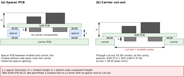
Mounting options (a) spacer PCB and (b) carrier cut-out (cross-section, not to scale)
- Option (a), spacer PCB. A spacer PCB sits between the module and the carrier, so that the module's bottom-side components clear the carrier inside the spacer opening. The spacer is soldered on both faces: the module LGA pads are soldered to the spacer, and the spacer is soldered to the carrier. The carrier keeps the area under the module cavity free of components, at the cavity outline given for option (b).
- Option (b), carrier cut-out. The carrier has a through cut-out the size of the module's central cavity, at the cavity position, with R1.00 corners. The module pads solder to the carrier pads around it. Figure 6 and Figure 7 show the cut-out in the land pattern.
| Attribute | E1M | E1M-X |
|---|---|---|
| Size | 27.0 mm across × 29.0 mm down | 57.45 mm across × 39.45 mm down |
| Corner radius | R1.00 | R1.00 |
| Position, from the outline left edge | 4.0 mm | 3.775 mm |
| Position, from the outline top edge | 3.0 mm | 2.775 mm |
| Source | module cavity, E1M-STD §4.1, §5.1.1 | module cavity, E1M-STD §4.2, §5.1.2 |
The cut-out is centred in the outline, so its distances from the right and bottom edges equal those from the left and top edges. The spacer thickness, the maximum module height and the maximum bottom-side component height are TBD in the specification (E1M-STD §5.2), so the enclosure clearance above the module is not yet known. The module documents still use the height-class terms: HG-V2N-M1-001 states standard height, with the DX-M1, its LPDDR5X and its SPI NAND as top-side parts; DS-AEN-001 and DS-V2N-001 state no class (Annex C, C-34). These statements do not change the rule below.
| ID | Rule | Strength | Source |
|---|---|---|---|
| CB-MEC-09 | Mount every module with option (a), a spacer PCB between module and carrier, soldered on both faces (module to spacer, spacer to carrier), or option (b), a through cut-out in the carrier the size of the module cavity, at the cavity position, with R1.00 corners (E1M 27.0 mm across × 29.0 mm down, 4.0 mm from the left and 3.0 mm from the top outline edge; E1M-X 57.45 mm across × 39.45 mm down, 3.775 mm from the left and 2.775 mm from the top outline edge). Do not solder a module directly on a carrier without either. With either option, place no carrier component inside the cavity outline. | MUST | E1M-STD §5.2 as changed by Alp Lab, 2026-10-19 |
3.5 Soldering and Reflow
Modules are soldered with an LGA-class reflow process (E1M-STD §5.4). §5.4.1 gives a recommended reflow profile (informative, measured on E1M-AEN with ALPHA OM338 SAC paste); a profile for the other reference modules is not specified there. E1M-AEN, E1M-X V2N and E1M-X V2N-M1 publish the same lead-free profile: the E1M-AEN measured profile, on a JTR1000 convection oven with ALPHA OM338 SAC paste, which the E1M-X datasheets give as the recommended starting profile (DS-AEN-001, DS-V2N-001, DS-V2N-M1-001 "Reflow Profile"). Figure 9 shows one measured curve with its values; the table gives the recommended window and the measured ranges. The SAC liquidus is 217 °C.
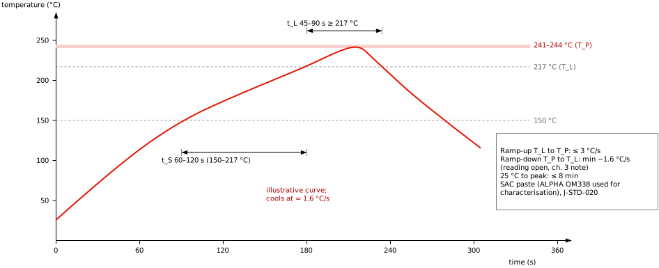
Measured reflow profile of the E1M-AEN (JTR1000 oven, ALPHA OM338)
| Parameter | Window min | Window max | Measured | Unit |
|---|---|---|---|---|
| Preheat time, 30–150 °C | 60 | 160 | 116.5–122.0 | s |
| Soak time, 150–217 °C | 60 | 120 | 70.5–73.5 | s |
| Time at or above 220 °C | 45 | 90 | 56.5–60.0 | s |
| Cooling slope from 220 °C | −4 | −0.5 | −1.53 to −1.66 | °C/s |
| Peak package temperature | 230 | 250 | 240.9–244.3 | °C |
The cooling window is a signed slope from 220 °C, −4 to −0.5 °C/s: cool at least 0.5 °C/s and no faster than 4 °C/s. The measured E1M-AEN run cooled at −1.53 to −1.66 °C/s.
- Profile the oven with a thermocouple on the module, at the centre of the pad field, on the populated carrier.
- Rework and desoldering guidance is not specified in E1M-STD-1.0 revision 1.4; treat a removed module as scrap.
- Inspect the hidden LGA joints with X-ray on first articles.
| ID | Rule | Strength | Source |
|---|---|---|---|
| CB-MEC-10 | Reflow the module within the common profile above, with SAC paste. | MUST | E1M-STD §5.4; DS-AEN-001, DS-V2N-001, DS-V2N-M1-001 Reflow Profile |
| CB-MEC-11 | Place the module on the carrier side that is reflowed last, top side up; do not pass a mounted module through a second reflow upside down. | SHOULD | Guide (informative) |
| CB-MEC-12 | X-ray inspect the module joints on first articles and after any process change. | SHOULD | Guide (informative) |
3.6 Handling, Moisture and Packaging
- ESD. Modules are ESD-sensitive; handle them on grounded equipment (HG-AEN-001, HG-V2N-001).
- Moisture. Modules are classified per IPC/JEDEC J-STD-020; the MSL, floor life and bake conditions are TBD in every module datasheet. Handle dry-packed modules per J-STD-033 and bake before reflow when the floor life is exceeded.
- Mechanical stress. Avoid bending or impact after soldering. The carrier flatness limit is TBD (HG-V2N-001); keep the module area free of mounting holes and stiffener edges that bend the board under the module. A heatsink or fan bracket rests on the carrier or the enclosure, not on the solder joints (Chapter 21).
- Packaging. Modules are supplied in JEDEC matrix trays: E1M-AEN, E1M-X V2N and E1M-X V2N-M1 (DS-AEN-001, DS-V2N-001, DS-V2N-M1-001 Packaging).
| ID | Rule | Strength | Source |
|---|---|---|---|
| CB-MEC-13 | Store and handle modules per J-STD-033 at the MSL the module datasheet states; bake per the datasheet when the floor life is exceeded. | MUST | DS-AEN-001, DS-V2N-001 MSL & Handling |
| CB-MEC-14 | Do not load the module joints mechanically: no heatsink, cable or enclosure force carried by the module. | MUST | HG-AEN-001, HG-V2N-001 Handling and Assembly |
| CB-MEC-15 | Plan the assembly line for tray feeding of the module (JEDEC matrix tray, every module). | SHOULD | DS-AEN-001, DS-V2N-001, DS-V2N-M1-001 Packaging |
| CB-MEC-16 | Rate carrier parts, and declare the product, for the ambient range of the supported SoM set: − 40 to +75 °C for a carrier that hosts any module. | SHOULD | DS-AEN-001, DS-V2N-001 Operating Conditions |
3.7 Per-Module Differences
| Item | E1M-AEN | E1M-X V2N | E1M-X V2N-M1 |
|---|---|---|---|
| Module length × width | 34.9– 35.1 × 34.9– 35.1 mm | 64.9– 65.1 × 44.9– 45.1 mm | 64.9– 65.1 × 44.9– 45.1 mm |
| Pad pitch | 1.0 mm | 1.00 mm (DS-V2N-001 0.10) | 1.00 mm (DS-V2N-M1-001 0.13) |
| Pad size | 0.40 mm round, NSMD | ⌀ 0.40 mm round, NSMD; one pad size (DS-V2N-001 0.10) | ⌀ 0.40 mm round, NSMD; one pad size (DS-V2N-M1-001 0.13) |
| Solder-mask opening | 0.50 mm | ⌀ 0.50 mm (NSMD) | ⌀ 0.50 mm (NSMD) |
| Stencil thickness | 0.08 mm | 80 μm | 80 μm |
| Height class in the module documents (replaced by the mounting options) | not stated | not stated | standard |
| Module height, mass | TBD, TBD | TBD, TBD | TBD, TBD |
| Under-module carrier keep-out | no components inside the pad ring | no components taller than TBD mm | no components taller than TBD mm |
| Packaging | JEDEC matrix tray | JEDEC tray | JEDEC tray |
| MSL, floor life, bake | TBD | TBD | TBD |
| Ambient operating temperature | − 40 to +75 °C | − 40 to +85 °C | − 40 to +85 °C |
| Storage temperature | − 40 to +125 °C | − 40 to +125 °C | − 40 to +125 °C |
3.8 Chapter Checklist
| Check | Item | Rule |
|---|---|---|
| ☐ | Land pattern placed from the pinout JSON; A1 matches. | CB-MEC-01 |
| ☐ | E1M: 1.0 mm pitch, 0.40 mm round pads. | CB-MEC-02 |
| ☐ | Footprint built in the pad frame of Chapter 1 (letters = rows, top to bottom; numbers = columns, left to right; E1M-X landscape) from the pinout JSON; E1M-X 1.00 mm pitch, ⌀ 0.40 mm pads per DS-V2N-001 0.10 / DS-V2N-M1-001 0.13. | CB-MEC-01, CB-MEC-03 |
| ☐ | NSMD pads, mask opening and stencil per the land-pattern table. | CB-MEC-04 |
| ☐ | No components inside the pad ring. | CB-MEC-05 |
| ☐ | Courtyard of 2.0 mm round the outline kept clear (E1M 39.0 × 39.0 mm; E1M-X 69.0 mm across × 49.0 mm down). | CB-MEC-06 |
| ☐ | Top-layer traces between module pads mask-covered; none across an option (b) cut-out. | CB-MEC-07 |
| ☐ | A1 mark and local fiducials on the carrier. | CB-MEC-08 |
| ☐ | Spacer PCB (option a, soldered on both faces) or carrier cut-out (option b) present; a cut-out at the cavity size and position, R1.00 corners; no carrier components inside the cavity outline under either option. | CB-MEC-09 |
| ☐ | Oven profiled to the common reflow limits; module reflowed last, top side up. | CB-MEC-10, CB-MEC-11 |
| ☐ | First-article X-ray of the module joints. | CB-MEC-12 |
| ☐ | MSL handling and bake procedure in the assembly instructions. | CB-MEC-13 |
| ☐ | No mechanical load on the module joints. | CB-MEC-14 |
| ☐ | Tray feeding planned. | CB-MEC-15 |
| ☐ | Carrier parts rated for the SoM-set ambient range. | CB-MEC-16 |
4 PCB Stack-up and Controlled-Impedance Routing
This chapter sets the layer stack, the ground connection of the module and the impedance and skew targets for every high-speed interface. The interface chapters (11 to 19) add the circuit around each pair.
4.1 Layer Count and Stack-up
A 4-layer carrier is the minimum for E1M; 6 layers ease escape routing and give each high-speed pair a cleaner reference (HG-AEN-001 "Layer Stack-Up"). An E1M-X carrier that uses PCIe, both gigabit Ethernet ports and four-lane CSI-2 needs a second high-speed routing layer between ground planes, so 6 layers are recommended. Figure 10 shows two reference stacks.
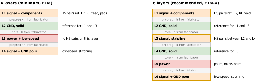
Reference 4-layer and 6-layer stack-ups
- 4 layers. L1 carries the module pads, the high-speed escapes and the RF feed, referenced to the solid ground plane L2. L3 carries power pours and low-speed signals only. L4 carries low-speed signals and a ground pour stitched to L2.
- 6 layers. L1 and L3 carry high-speed pairs; L3 is a stripline layer between ground planes L2 and L4. L5 carries the power pours and L6 the low-speed signals with a ground pour.
- The dielectric heights, trace widths and gaps come from the fabricator's impedance calculator for the chosen material; no stack-up dimension in this guide is normative.
| ID | Rule | Strength | Source |
|---|---|---|---|
| CB-PCB-01 | Use at least 4 layers for an E1M carrier and at least 6 layers for an E1M-X carrier that routes PCIe, both Ethernet ports or four-lane CSI-2. | SHOULD | HG-AEN-001 Layer Stack-Up; Guide |
| CB-PCB-02 | Set dielectric heights and trace geometry with the fabricator's impedance calculator; order the board impedance-controlled, with test coupons for each impedance class. | SHOULD | HG-AEN-001 Controlled-Impedance Routing; Guide |
4.2 Ground Connection of the Module
Every GND pad is a return path and a heat path. E1M has 49 GND pads and E1M-X has 105 (E1M-STD §7.3.1; the full lists are in pinout/v1.json and pinout/x-v1.json). The specification requires a low-impedance plane connection (E1M-STD §9.2 (3)). E1M-AEN thermal data assume all 49 pads soldered, each with at least one via to a solid plane (DS-AEN-001 "Thermal Characteristics"). The E1M-X V2N guide asks for a solid ground plane under the whole module footprint (HG-V2N-001).
| ID | Rule | Strength | Source |
|---|---|---|---|
| CB-PCB-03 | Connect every GND pad of the module to a low-impedance ground plane. | MUST | E1M-STD §7.3.1, §9.2 (3) |
| CB-PCB-16 | Give every GND pad at least one via to the plane, as the E1M-AEN thermal data assume. | SHOULD | DS-AEN-001 Thermal Characteristics |
| CB-PCB-04 | Keep the ground plane next to the top layer (L2) solid under the whole module footprint; route nothing on L2 inside the outline. | SHOULD | HG-V2N-001 Power Design Guidelines |
The 5 V and VIO_OUT pads need wide copper and their own via counts; Chapters 5 and 6 give them.
4.3 Impedance and Skew Targets
The table gives the target for each interface, using the strictest value of the module documents. Skew is in picoseconds; convert it to length with the propagation delay of the actual stack-up from the fabricator.
| Interface | Impedance | Tolerance | Intra-pair skew | Group matching | Source |
|---|---|---|---|---|---|
| Ethernet MDI | 100 Ω differential | ± 10 % | ≤ ± 2 ps | across the four pairs of a port: TBD | E1M-STD §7.3.6 (1); HG-AEN-001; HG-V2N-001 |
| USB 2.0 | 90 Ω differential | ± 10 % | ± 2 ps | — | HG-V2N-001 (E1M-AEN: ≤ ± 5 ps) |
| USB 3.x SuperSpeed | 85 Ω differential | not stated | ± 2 ps | TX and RX pairs of a port independent | HG-V2N-001 |
| PCIe | 85 Ω differential | not stated | ± 2 ps (HG-V2N-001) | lane to lane ± 2 ps (HG-V2N-M1-001); E1M-X V2N-M1 adds the on-module multiplexer skew, TBD | HG-V2N-001; HG-V2N-M1-001 |
| MIPI CSI-2, DSI | 100 Ω differential | ± 10 % | ± 2 ps (Guide, informative) | clock matched to the data lanes of the group as closely as the layout allows (Guide, informative) | HG-AEN-001; HG-V2N-001; Guide |
| Antenna feed | 50 Ω single-ended | ± 10 % | — | — | E1M-STD §7.3.2; HG-AEN-001 |
The 90 Ω in DS-V2N-001 applies to the USB 2.0 D± pairs (USB0_30_D_P/N, USB2_20_P/N); HG-V2N-001 gives 85 Ω for the USB 3.2 SuperSpeed pairs and 90 Ω for USB 2.0, so the documents agree. Module documents give no numeric skew for MIPI lanes and no group skew for Ethernet; the MIPI values in the table are this guide's informative targets.
| ID | Rule | Strength | Source |
|---|---|---|---|
| CB-PCB-05 | Route the antenna feed as a 50 Ω controlled-impedance trace. | MUST | E1M-STD §7.3.2 |
| CB-PCB-06 | Route every Ethernet MDI pair as a 100 Ω differential pair. | MUST | E1M-STD §7.3.6 (1) |
| CB-PCB-07 | Route the other high-speed interfaces to the impedance, tolerance and skew targets of the table above. | SHOULD | HG-AEN-001, HG-V2N-001, HG-V2N-M1-001, DS-V2N-001 |
| CB-PCB-08 | Match the two lines of each pair first, then the pairs of a group. Correct a mismatch close to where it starts (at the bend or pad that creates it), not at the far end. | SHOULD | HG-AEN-001; Guide |
| CB-PCB-09 | On an E1M-X carrier that supports V2N-M1, keep the PCIE0_* lane-to-lane skew within ± 2 ps and leave margin for the on-module multiplexer skew (TBD). | SHOULD | HG-V2N-M1-001 |
4.4 Escape Routing
Each interface group sits on one edge of the pad band. Route it out of that edge, on L1 or on a stripline layer, and keep the space under the module for low-speed nets. Figure 11 and Figure 12 show the groups, coloured by pad class from the pinout JSON. The edges are named in the top view of Chapter 1: rows A, B along the top edge, the last two rows along the bottom edge, columns 1– 3 along the left edge and the last three columns along the right edge.
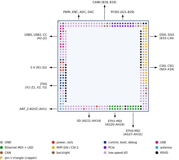
E1M pad classes and escape directions (top view)
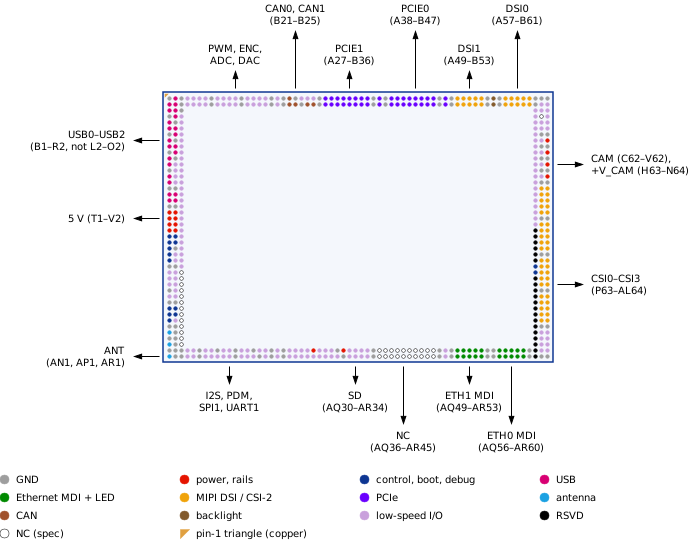
E1M-X pad classes and escape directions (top view)
| Edge | E1M | E1M-X |
|---|---|---|
| Left (columns 1– 3) | USB0 B1–G1, C2, D2; USB2 I1, J1, I2, J2; USB_CC1, USB_CC2 A2, B2; UART0 F2, G2; SPI0 L1, M1, N1, M2, N2; IO0 L2; MODULE_EN O1; MODULE_STBY O2; VIO_OUT P1, P2; VDD R1, R2, S1, S2; boot straps U1, U2, V1, V2; PORn W1; IO2 W2; JTAG X1, Y1, Z1, X2, Y2; AUDIO_CLK Z2; PDM AA1, AB1, AA2, AB2; I2C0 AD2, AE2; IO3 AG2; antenna AD1, AF1, AH1; column 3: PWM6, PWM7 A3, B3, IO13, IO15–IO25 E3–P3, RSVD Q3–AC3, DBG_TX, DBG_RX AD3, AE3 | USB0 B1, C1, E1, F1, H1, I1, C2, D2; USB2 F2, G2, I2, J2; USB1 K1, L1, N1, O1, Q1, R1, Q2, R2; USB_CC1, USB_CC2 A2, B2; IO0–IO3 L2–O2; VDD_5V_IN T1–V2; VIO_OUT W1, W2; boot straps X1, X2, Y1, Y2; PORn Z1; MODULE_EN AA1; MODULE_STBY AB1; UART0 AA2, AB2; SPI0 AD1, AE1, AF1, AD2, AE2; IO4, IO5 AF2, AG2; I2C0 AH1 (SCL), AH2 (SDA); JTAG AJ1, AK1, AL1, AJ2, AK2; IO6 AL2; antenna AN1, AP1, AR1; LCD D3–AC3; spec-NC AD3–AP3 |
| Right (columns 32– 34 / 62– 64) | RSVD A33, A34, D32–R32, AG32, AH32; parallel camera S32–AD32; DSI0 B33–F34; DSI1 H33–L34; CSI0 N33–R34; CSI1 T33–X34; CAM_VFB0, +V_CAM0 Z33, Z34; CAM_VFB1, +V_CAM1 AB33, AB34; I2S0 AD33–AE34; IO7–IO10 AG33, AG34, AH33, AH34 | parallel camera C62–V62; RSVD W62–AB62, AE62–AR62; DBG_TX, DBG_RX AC62, AD62; SPI2 B63, C63, B64, C64, D64; spec-NC D63; I2C2 E63, E64; IO25, IO26 F63, F64; CAM_VFB0–CAM_VFB3, +V_CAM0–+V_CAM3 H63–N64; CSI0 P63–T64; CSI1 V63–Z64; CSI2 AB63–AF64; CSI3 AH63–AL64; IO27–IO34 AN63–AQ64 |
Top (rows A, B) | PWM A4–B6 (and A3, B3); encoder A7–B10; ADC A12–B15; DAC A16, B16; IO11 A18; CAN_STBY A19; CAN0 B18, B19; PCIE0 A21–B29; backlight A31, B31 | PWM A4–B7; encoder A9–B12; ADC A14–B17; DAC A19, B19; CAN_STBY A21; CAN0 B21, B22; CAN1 B24, B25; I2C3 A23, A24; IO35 A25; PCIE1 A27–B36; PCIE0 A38–B47; DSI1 A49–B53; backlight A55, B55; DSI0 A57–B61 |
Bottom (rows AG, AH / AQ, AR) | UART1 AG4, AH4; I3C AG5, AH5; I2S1 AG6–AH7; SPI1 AG8–AG10, AH8, AH9; SD_VDD AH10; SD AG11–AG14, AH11–AH14; +S_CAP AG15; IO4–IO6 AG16, AH18, AG18; RTC_CLKOUT AH16; I2C1 AG17, AH17; ETH1 AG20–AH24; RSVD AG26, AH26; ETH0 AG27–AH31 | I2S0 AQ4, AQ5, AR4, AR5; PDM AQ7, AQ8, AR7, AR8; AUDIO_CLK AR9; I2S1 AQ10, AQ11, AR10, AR11; SPI1 AQ13, AQ14, AR13–AR15; RTC_CLKOUT AQ16; UART1 AQ17, AR17; I3C AQ19, AR19; IO8–IO24 AQ21–AR29 (except AQ25); +S_CAP AQ25; SD_VDD_OUT AQ30; SD AQ31–AR34; spec-NC AQ36–AR45; I2C1 AQ47, AR47; ETH1 AQ49–AR53; ETH0 AQ56–AR60 |
- Escape all four pairs of every Ethernet port the carrier uses, even if a supported module uses only
DAandDB(E1M-STD §7.3.6 (3), Chapter 11). - E1M-X has pads whose default function in the specification is
NC:D63,AD3–AP3,AQ36–AQ45andAR36–AR45. A carrier MAY route through them or leave them open (E1M-STD §7.3.4). E1M has noNCpads. - A pad that a module datasheet calls "NC" is not a spec-
NCpad: never route a foreign net through it (CB-ANY-19). Never touch anRSVDpad (CB-ANY-18).
DS-V2N-001 "Not Connected Pins" lists the spec-NC pads AD3–AP3, AQ36–AQ45 and AR36–AR45 as "must be left floating", which conflicts with the permission of E1M-STD §7.3.4 to route through them. The conflict is listed in Annex C. On a carrier that supports E1M-X V2N or V2N-M1, confirm with Alp Lab before routing a carrier net through a spec-NC pad.
| ID | Rule | Strength | Source |
|---|---|---|---|
| CB-PCB-10 | Route each high-speed group out of the edge it sits on, on L1 or on a stripline layer between ground planes; do not route high-speed pairs across the module to another edge. | SHOULD | Guide (informative) |
| CB-PCB-11 | Carrier nets MAY pass through the E1M-X spec-NC pads D63, AD3–AP3, AQ36–AQ45, AR36–AR45, and through no other module pad. On a carrier that supports E1M-X V2N or V2N-M1, get Alp Lab confirmation first (DS-V2N-001 asks for these pads to be left floating). | MAY | E1M-STD §7.3.4; DS-V2N-001 Not Connected Pins |
4.5 Layer Changes, Vias and Reference Planes
Figure 13 shows the three layout faults that most often break a high-speed pair.
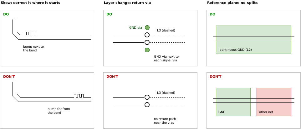
Differential-pair layout: skew correction, layer change, reference plane
- Keep high-speed pairs short and direct, and use as few vias as possible; every via is an impedance step.
- At a layer change, place a ground via next to each signal via, so the return current can change planes with the signal (HG-AEN-001).
- Avoid stubs: no test points or branches on high-speed pairs, and use the full via length (or back-drilled vias) for PCIe and USB 3.x.
- Never let a pair cross a split or a gap in its reference plane; the return current has no path and emissions and crosstalk rise (HG-AEN-001).
| ID | Rule | Strength | Source |
|---|---|---|---|
| CB-PCB-12 | Place a ground stitching via next to every signal via of a high-speed pair at a layer change. | SHOULD | HG-AEN-001 Controlled-Impedance Routing |
| CB-PCB-13 | Do not route a differential pair across a split or gap in its reference plane, and do not reference high-speed pairs to a power-only layer. | SHOULD NOT | HG-AEN-001 Layer Stack-Up |
| CB-PCB-14 | Keep high-speed pairs free of stubs: no test points or branches; full-length or back-drilled vias for PCIe and USB 3.x. | SHOULD | HG-AEN-001; Guide |
4.6 Noise Segregation
Switching regulators, their inductors and their high-current loops couple into the RF feed, the analogue inputs, the MIPI lanes and the audio clocks. Place them away from these nets, keep their loops small on the layer next to a ground plane, and keep a ground area between them and the sensitive nets (HG-AEN-001).
| ID | Rule | Strength | Source |
|---|---|---|---|
| CB-PCB-15 | Keep switching power stages and high-current paths away from the antenna feed, the ADC inputs, the MIPI lanes and the audio clock nets, separated by ground. | SHOULD | HG-AEN-001; DS-AEN-001 Keep-Out Zones |
4.7 Per-Module Differences
| Item | E1M-AEN | E1M-X V2N | E1M-X V2N-M1 |
|---|---|---|---|
| Ethernet | ETH0 DA, DB only (100 Mbps) | ETH0 and ETH1, four pairs each (1 Gbps) | as E1M-X V2N |
| USB | USB 2.0 high speed on B1 / C1; no SuperSpeed | USB0 SuperSpeed + D±; USB2 D±; USB1 not routed | as E1M-X V2N |
| PCIe | not routed | PCIE0 lanes 0– 1, Gen3 | PCIE0 lanes 0– 1, multiplexed with the on-module DX-M1 (skew TBD); the stock image routes them to the DX-M1 on every boot, so a carrier PCIE0 device is not reachable (HG-V2N-M1-001) |
| MIPI DSI | DSI0, 2 lanes | DSI0, 4 lanes | DSI0, 4 lanes |
| MIPI CSI-2 | CSI0, 2 lanes | CSI0, CSI1, 4 lanes each | CSI0, CSI1, 4 lanes each |
| Antenna feeds | AH1 (2.4 GHz) | AR1 | AR1 |
| USB 2.0 intra-pair skew in module guide | ≤ ± 5 ps | ± 2 ps | ± 2 ps |
| USB 3.2 SuperSpeed impedance in module guide | — (not routed) | 85 Ω | 85 Ω |
GND pads | 49 | 105 | 105 |
4.8 Chapter Checklist
| Check | Item | Rule |
|---|---|---|
| ☐ | Layer count chosen (≥ 4 for E1M, ≥ 6 for a full E1M-X carrier). | CB-PCB-01 |
| ☐ | Stack-up and trace geometry from the fabricator; impedance-controlled order with coupons. | CB-PCB-02 |
| ☐ | Every GND pad on the plane, with at least one via each; L2 solid under the module. | CB-PCB-03, CB-PCB-16, CB-PCB-04 |
| ☐ | Antenna feed 50 Ω; MDI pairs 100 Ω differential. | CB-PCB-05, CB-PCB-06 |
| ☐ | Other pairs to the impedance and skew table; intra-pair matched first, corrected near the source. | CB-PCB-07, CB-PCB-08 |
| ☐ | V2N-M1 PCIE0 lane-to-lane skew and multiplexer margin. | CB-PCB-09 |
| ☐ | Groups escape on their own edge; only spec-NC pads used for pass-through. | CB-PCB-10, CB-PCB-11 |
| ☐ | Ground via at every high-speed layer change; no plane-split crossings; no stubs. | CB-PCB-12, CB-PCB-13, CB-PCB-14 |
| ☐ | Switching power stages separated from RF, analogue, MIPI and audio clocks. | CB-PCB-15 |
5 5 V Input Stage
A conformant SoM takes one supply from the carrier: 5 V on its VDD_5V_IN pads. The SoM generates and sequences every internal rail itself (E1M-STD §6.1, §6.2). The carrier's job is to deliver that 5 V inside a tight window at the pads, protect the SoM from everything outside the window, and keep enough energy next to the pads for the SoM to shut down cleanly when the supply goes away.
This chapter gives one input stage that works with every conformant E1M and E1M-X SoM. The window it uses is the strictest combination of the reference SoMs, as fixed by E1M-STD-1.0 revision 1.4 §6.1.1.
5.1 Supply Contract
| Item | E1M | E1M-X |
|---|---|---|
| Pad name (silkscreen) | VDD | VDD_5V_IN |
| Pads | R1, R2, S1, S2 (4 pads) | T1, T2, U1, U2, V1, V2 (6 pads) |
| Ground pads | 49 (pinout/v1.json) | 105 (pinout/x-v1.json) |
| Other power inputs | none (+S_CAP is an RTC backup-store connection, not a power input; a carrier charger may feed it per the SoM manifest, chapter 10) | none (as E1M) |
In this guide VDD_5V_IN means both names. Each form factor has its own pad coordinates, and the same pad ID can carry a different signal on the other form factor: E1M-X 5 V pads U1, U2, V1, V2 are the E1M boot-strap pads BOOT2, BOOT1, BOOT3, BOOT0, and E1M 5 V pads R1, R2 are E1M-X USB1_30_TX0_N, USB1_30_ID (E1M S1, S2 are E1M-X GND). A carrier footprint is for one form factor only; never copy a 5 V net assignment from one form factor to the other.
5.2 Design Window at the Pads
The window applies at the VDD_5V_IN pads, not at the regulator output or the input connector. Every drop between the source and the pads (connector, protection, eFuse, OR-ing element, current-sense shunt, copper) comes out of it.
| ID | Level | Rule | Source |
|---|---|---|---|
| CB-PWR-01 | MUST | Hold the voltage at the VDD_5V_IN pads between 4.75 V and 5.25 V at every load from zero up to the peak input current the SoM declares. | E1M-STD §6.1.1 (1) |
| CB-PWR-02 | MUST | Keep the voltage at the pads at or below 5.5 V at all times: steady state, load release, hot-plug overshoot and surge. | E1M-STD §6.1.1 (2) |
| CB-PWR-03 | MUST | Make the rise from 0 V to 4.75 V monotonic, and complete it within 40 ms. | E1M-STD §6.1.1 (3) (value: E1M-AEN only) |
| CB-PWR-04 | MUST | Connect every VDD_5V_IN pad to the 5 V supply through a low-impedance path. Connect no other supply to these pads. | E1M-STD §6.1.1 (4) |
| CB-PWR-05 | MUST | Supply only VDD_5V_IN. Never drive, back-feed or connect a carrier supply to any SoM output rail (VIO_OUT, SD_VDD / SD_VDD_OUT, +V_CAMx, BL_LED_A); see chapter 6. | E1M-STD §6.1, §6.7.1 |
| CB-PWR-43 | MUST | Feed VDD_5V_IN from a USB VBUS (USB-C, USB Type-A, USB PD) only through a regulator (buck-boost, or PD negotiation to 9 V or more plus a buck to 5.0–5.1 V) whose output meets CB-PWR-01 and CB-PWR-02 at the pads. Never connect VBUS directly to the input stage of the pads. | E1M-STD §6.1.1 (1), (2); HG-AEN-001 |
| CB-PWR-06 | MAY | Use a wider window only in a carrier build that declares a SoM set whose manifests all declare that wider window. | E1M-STD §6.1.1, §8.4, §9.2 |
USB VBUS is specified down to 4.75 V at the source and drops further in the cable and receptacle, and a USB-C / PD source can deliver up to 5.5 V at vSafe5V. Neither fits a 4.75–5.25 V window after the drops of the protection chain, and a 5.3–5.5 V source can trip a correctly set OVP (CB-PWR-10). The E1M-EVK therefore runs its USB-PD input through an eFuse and a buck regulator to its 5 V rail.
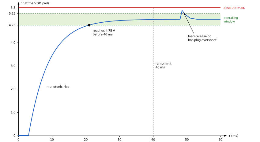
5 V design window at the pads: monotonic rise to 4.75 V within 40 ms, operation within 4.75–5.25 V, and every overshoot below 5.5 V
The 4.75–5.25 V window and the 5.5 V absolute maximum are tighter than the E1M-X V2N / V2N-M1 datasheets (4.5–5.5 V, 6.0 V absolute maximum). A carrier that targets "any conformant SoM" uses the tighter values. The 40 ms ramp is confirmed only for E1M-AEN but binds every carrier until a later spec revision states otherwise (E1M-STD §6.1, value-provenance note).
5.3 Protection Chain
A conformant SoM is not required to have input protection, and the reference SoMs have none. The carrier provides the whole chain, in this order from the connector:
- TVS at the connector, which absorbs surge energy and protects the parts behind it.
- Reverse-polarity protection, where the 5 V connector can be mis-wired.
- Over-voltage cut-off and inrush control: an eFuse or load switch with an over-voltage cut-off (OVP), a controlled output slew and a current limit.
- Hold-up capacitance next to the
VDD_5V_INpads.
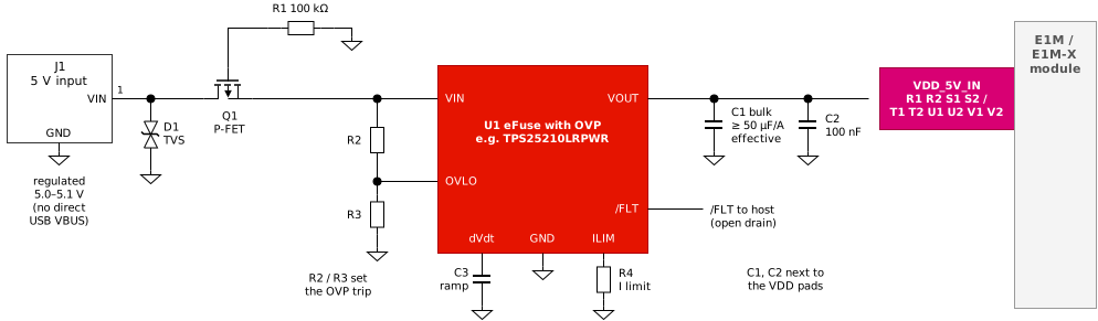
Reference 5 V input stage from a regulated 5.0–5.1 V source: TVS D1, reverse-polarity P-FET Q1, eFuse U1 with OVP divider R2/R3, ramp capacitor C3 and current-limit resistor R4, hold-up C1 and C2 at the VDD_5V_IN pads
The example eFuse part is the one used on an earlier E1M-EVK revision and is sized for an E1M carrier. Before reusing it, check its current-limit range against the budget (E1M-X: at least 5 A peak plus the carrier loads, CB-PWR-17) and its input absolute maximum against the TVS clamp voltage at the rated surge current (CB-PWR-09).
A TVS alone does not keep VDD_5V_IN at or below 5.5 V: a 5 V TVS clamps well above 6 V at its rated surge current.
| ID | Level | Rule | Source |
|---|---|---|---|
| CB-PWR-07 | MUST | Place an over-voltage cut-off or clamp (eFuse or load switch with OVP) between the 5 V source and the pads, so that CB-PWR-02 holds for every input event the product can see. | E1M-STD §6.1.1 (2), (6) |
| CB-PWR-08 | MUST | Fit reverse-polarity protection where the 5 V input connector can be mis-wired (barrel jack, screw terminal, wire-to-board). | E1M-STD §6.1.1 (6) |
| CB-PWR-09 | SHOULD | Place a TVS at the input connector, ahead of the OVP stage, with a short ground return. Choose the eFuse so that its input absolute maximum is above the TVS clamp voltage at the rated surge current. | HG-AEN-001; Guide (informative) |
| CB-PWR-10 | SHOULD | Set the OVP trip so that its whole tolerance band lies above the highest normal source voltage and its upper limit, plus the response overshoot of the OVP stage, stays at or below 5.5 V (see below). | Guide (informative) |
| CB-PWR-11 | MUST | Limit inrush with a controlled output slew sized for the SoM input capacitance plus the carrier hold-up capacitance, so that the ramp stays monotonic and reaches 4.75 V within 40 ms (CB-PWR-03). | E1M-STD §6.1.1 (3); HG-AEN-001 |
| CB-PWR-12 | SHOULD | Set the eFuse current limit above the inrush current plus the SoM start-up current. A current limit that trips during the ramp makes the ramp non-monotonic. | Guide (informative) |
| CB-PWR-13 | MUST | Where the carrier generates 5 V from a higher input voltage, keep the converter's load-release overshoot at the pads at or below 5.5 V. | E1M-STD §6.1.1 (2) |
| CB-PWR-14 | SHOULD | Where a converter failure (for example a shorted high-side switch) can put its input voltage on its output, keep an OVP stage between the converter and the pads. | Guide (informative) |
5.3.1 Setting the Over-voltage Trip
The OVP trip has to fit between the highest normal voltage and the 5.5 V absolute maximum. With Vsrc,max the highest source voltage at the OVP input (including the source's own load-release overshoot), Vtrip,min and Vtrip,max the tolerance band of the trip point (threshold accuracy plus divider tolerance) and ΔVresp the rise of the output during the response time of the OVP stage:
Vsrc,max < Vtrip,min and Vtrip,max + ΔVresp ≤ 5.5 V
Worked example (calculated, not a part recommendation): a 5.10 V source with ± 1.5 % tolerance gives Vsrc,max = 5.18 V. A trip point set to 5.36 V with ± 1 % total tolerance gives 5.31–5.41 V. That leaves 0.13 V above the source and 0.09 V for ΔVresp. The window is narrow: use a part with a tight OVP threshold and resistors of 0.1 % tolerance, and check ΔVresp against the part's response time and the capacitance on its output.
5.3.2 Setting the Ramp
With Ctotal the SoM input capacitance plus all carrier capacitance on the VDD_5V_IN node, an eFuse ramp time tramp (0 V to 5 V) gives an inrush current of
Iinrush = (Ctotal × 5 V) / tramp
Example (calculated): Ctotal = 50 μF (E1M-AEN on-module) + 100 μF (carrier) = 150 μF with tramp = 10 ms gives 75 mA. A ramp between about 5 ms and 20 ms leaves margin to the 40 ms limit and keeps inrush low.
5.4 Sizing the 5 V Source
Size the source for the peak current of everything on it, not the average. The SoM output rails (VIO_OUT, the SD-card supply and the camera supplies, chapter 6) are generated from VDD_5V_IN, and on E1M-AEN the on-module backlight driver runs directly from it. Count them unless the SoM manifest states that its declared peak already includes them.
| ID | Level | Rule | Source |
|---|---|---|---|
| CB-PWR-15 | MUST | Size the 5 V source for the peak input current the SoM declares plus every carrier load that shares the source. | E1M-STD §6.1.1 (5) |
| CB-PWR-16 | SHOULD | Fill in the budget worksheet below for every SoM the carrier targets and size the source, the eFuse current limit, the OR-ing element and the copper for the largest result. | Guide (informative) |
| CB-PWR-17 | SHOULD | E1M carriers: plan for at least 2 A peak at the VDD_5V_IN node. E1M-X carriers: plan for at least 5 A peak at the VDD_5V_IN node, plus the carrier loads on the same source. | Guide (informative); DS-AEN-001; HG-V2N-001, HG-V2N-M1-001 |
Load on the VDD_5V_IN node | Value | Current at 5.0 V |
|---|---|---|
SoM peak input current I_DDMAX (E1M-AEN801, calculated) | 834 mA | 834 mA |
| On-module backlight driver input (E1M-AEN, input current limit) | up to 520 mA | 520 mA |
SD_VDD card load | 3.4 V × 212 mA = 0.72 W | 170 mA |
+V_CAM0 + +V_CAM1 loads (LDOs from the 3.4 V domain) | 3.4 V × 170 mA = 0.58 W | 136 mA |
VIO_OUT load | 1.8 V × 100 mA = 0.18 W | 42 mA |
| Total at the pads | about 1.70 A |
The output-rail rows assume 85 % conversion efficiency inside the SoM (I = P / (0.85 × 5 V)); this is an assumption, not a module figure. DS-AEN-001 gives a 1.5 A peak source minimum and states that it covers the carrier loads on SD_VDD, VIO_OUT and the camera rails; this guide does not rely on that and adds them. Carrier loads that share the source but not the VDD_5V_IN node (3.3 V buck, USB host VBUS, displays) are added on top for the source and the input eFuse.
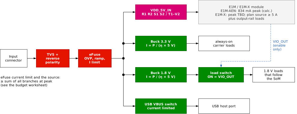
Carrier power tree: one protected 5 V node feeds the SoM and the carrier branches; carrier 1.8 V loads that follow the SoM sit behind a load switch enabled by VIO_OUT
5.5 Hold-up Capacitance
When 5 V is lost, the SoM needs time to put its SoC in reset in an orderly way. On E1M-AEN hw_rev R3 the on-module supervisor pulls PORn low and must finish before the 1.8 V I/O rail falls below 1.65 V; the hold-up capacitance on the carrier sets how fast 5 V collapses.
E1M-AEN hw_rev R2 has no on-module supervisor: a carrier that hosts R2 modules must hold the SoC in reset while its supply is below 1.65 V, or the SoC can be permanently damaged (E1M-AEN erratum E-02).
| ID | Level | Rule | Source |
|---|---|---|---|
| CB-PWR-18 | MUST | Place at least the bulk capacitance the SoM declares next to the VDD_5V_IN pads, after any eFuse, OR-ing element or current-sense shunt. For a carrier that targets any SoM, use the largest declared value. | E1M-STD §6.1.1 (7) |
| CB-PWR-19 | MUST | E1M: at least 50 μF effective per ampere of the total current drawn from the VDD_5V_IN node, plus 100 nF. Example: 1.70 A from the worksheet needs at least 85 μF effective. | E1M-STD §6.1.1 (7); DS-AEN-001, HG-AEN-001 |
| CB-PWR-20 | MUST | E1M-X: at least 10 μF plus 100 nF close to the VDD_5V_IN pads. | E1M-STD §6.1.1 (7); DS-V2N-001, DS-V2N-M1-001 |
| CB-PWR-21 | SHOULD | Count the effective capacitance at 5 V DC bias and at the lowest operating temperature. A ceramic capacitor can lose most of its nominal value at 5 V; a polymer capacitor keeps it. | HG-AEN-001; Guide (informative) |
| CB-PWR-22 | SHOULD | Where carrier loads on the same node make the hold-up capacitance large, isolate the SoM node from them with an ideal diode instead. | HG-AEN-001 |
| CB-PWR-23 | SHOULD | Add decoupling capacitors close to high-current carrier loads. | E1M-STD §6.1 |
The E1M-EVK (2641-R3) is a measurement board: it places a 0.1 Ω shunt permanently in the module supply and has only 0.10 μF on VDD_5V_IN. Do not copy these values into a product carrier.
5.6 Multiple Sources
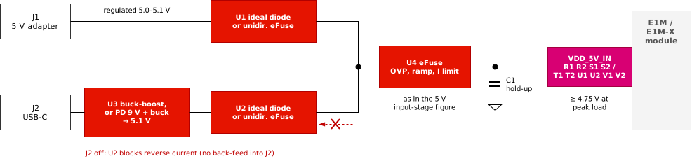
OR-ing two 5 V sources: the USB-C input is regulated to 5.1 V first, each source has its own ideal diode or unidirectional eFuse so the idle source is never back-fed, and the OR node passes through the OVP eFuse stage of the input-stage figure before the pads
| ID | Level | Rule | Source |
|---|---|---|---|
| CB-PWR-24 | MUST | Where VDD_5V_IN can be fed from more than one source, never back-feed an inactive source. Use an ideal-diode controller or a unidirectional eFuse per source. | E1M-STD §6.1.1 (8) |
| CB-PWR-25 | MUST | Keep at least 4.75 V at the pads at the peak load after the drop of the OR-ing element (CB-PWR-01). | E1M-STD §6.1.1 (8) |
| CB-PWR-26 | SHOULD | Do not OR with Schottky diodes: their forward drop from a 5.0 V source, or from a 4.75 V USB VBUS, leaves the pads below 4.75 V. | HG-AEN-001 |
| CB-PWR-44 | MUST | Keep the over-voltage cut-off of CB-PWR-07 between every source and the pads: one OVP eFuse after the OR node, or an OVP-capable unidirectional eFuse per source. | E1M-STD §6.1.1 (2), (6) |
| CB-PWR-27 | SHOULD | Define a priority between the sources, or make sure that the switch-over keeps the ramp and the window (CB-PWR-01 to CB-PWR-03) at the pads. | Guide (informative) |
5.7 Current-sense Shunts
A shunt in series with VDD_5V_IN takes its drop out of the window. A shunt sized for microampere standby measurements (hundreds of milliohms or more) drops too much at run current.
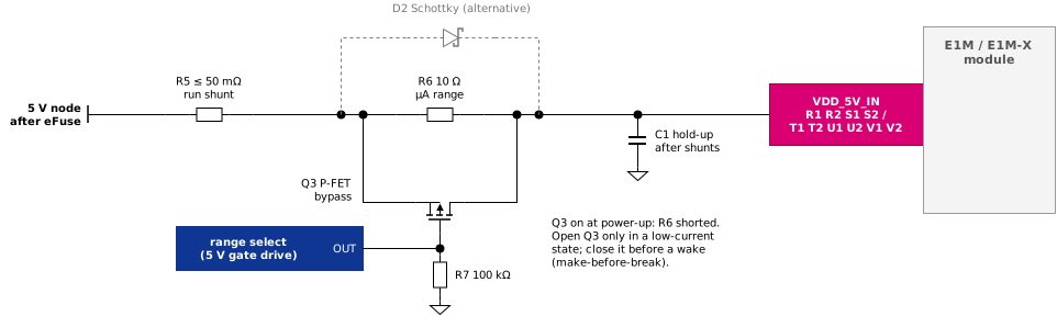
Two-range current measurement: a low-value run shunt R5 always in circuit, and a high-value range shunt R6 bypassed by Q3 by default (make-before-break)
| ID | Level | Rule | Source |
|---|---|---|---|
| CB-PWR-28 | MUST | Size every series element so that at least 4.75 V remains at the pads at the peak load (CB-PWR-01). | E1M-STD §6.1.1 (1) |
| CB-PWR-29 | SHOULD | Use a shunt of 50 mΩ or less for normal operation. | HG-AEN-001 |
| CB-PWR-30 | SHOULD | Bypass any high-value measurement shunt automatically: the bypass is closed at power-up, opens only while the SoM is in a known low-current state, and closes before a wake (make-before-break). A parallel Schottky diode is a simpler alternative that limits the drop to one forward voltage. | HG-AEN-001; Guide (informative) |
| CB-PWR-31 | SHOULD | Place the hold-up capacitance after the shunts (on the SoM side). | HG-AEN-001 |
5.8 Battery-powered Carriers
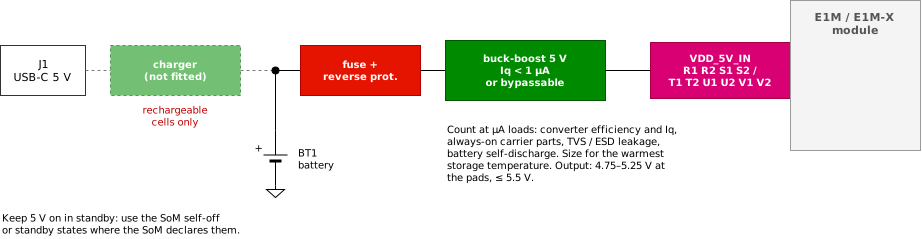
Battery power path: protection, a low-quiescent buck-boost converter to 5 V and the VDD_5V_IN pads; the charger is fitted only for rechargeable cells
| ID | Level | Rule | Source |
|---|---|---|---|
| CB-PWR-32 | MUST | Apply the full window to the converter output: CB-PWR-01 to CB-PWR-03 at the pads, over the whole battery voltage range. | E1M-STD §6.1.1 |
| CB-PWR-33 | SHOULD | Use a boost or buck-boost converter with sub-microampere quiescent current, or one that can be bypassed in standby. Count converter efficiency at microampere loads, the quiescent current of every always-on carrier part, TVS and ESD leakage and battery self-discharge. | HG-AEN-001 |
| CB-PWR-34 | SHOULD | Keep 5 V on in standby and use the low-power states that the SoM declares (for example self-off on E1M-AEN). Removing 5 V stops the SoM's always-on domain and its RTC, which then runs only from the backup store at +S_CAP (chapter 10). | HG-AEN-001 |
| CB-PWR-35 | MUST | Never charge a primary (non-rechargeable) cell, and never enable a charger with a primary cell fitted. | HG-AEN-001 (damage: leak, vent, burst) |
Charging a primary lithium cell can make it leak, vent or burst.
5.9 Switching 5 V Off
Chapter 8 gives the full power-down order. The 5 V input stage must support it:
| ID | Level | Rule | Source |
|---|---|---|---|
| CB-PWR-36 | SHOULD | Remove VDD_5V_IN only after VIO_OUT is low (the SoM is off). | E1M-STD §6.2.2 (4) |
| CB-PWR-37 | SHOULD | When power-cycling the SoM with 5 V, keep VDD_5V_IN off for at least 1 s before applying it again. Design power switches and auto-restart logic for this. | HG-AEN-001 (E1M-AEN, not yet characterised) |
Removing VDD_5V_IN gives the SoM firmware no notice, and writes to on-module non-volatile memory that are in progress are lost or corrupted.
5.10 Power Layout
| ID | Level | Rule | Source |
|---|---|---|---|
| CB-PWR-38 | MUST | Connect every GND pad of the SoM to a low-impedance ground plane. | E1M-STD §7.3.1, §9.2 (3) |
| CB-PWR-39 | SHOULD | Give every GND pad at least one via to the ground plane. | HG-AEN-001 |
| CB-PWR-40 | SHOULD | Join all VDD_5V_IN pads with one copper area on the top layer that leaves the module outline directly; the pads are on the outer row. Size the copper and the vias of the 5 V path for the peak current (E1M about 0.43 A per pad at 1.70 A; E1M-X about 0.83 A per pad at 5 A). | Guide (informative) |
| CB-PWR-41 | SHOULD | Keep the 5 V path from the eFuse to the pads short and wide, and place the hold-up capacitors next to the pads. | HG-AEN-001 |
| CB-PWR-42 | SHOULD | Place the TVS close to the input connector with a short ground return. | HG-AEN-001 |
5.11 Per-module Differences
| Parameter | E1M-AEN | E1M-X V2N | E1M-X V2N-M1 |
|---|---|---|---|
VDD_5V_IN pads | R1, R2, S1, S2 | T1, T2, U1, U2, V1, V2 | T1, T2, U1, U2, V1, V2 |
| Operating range (min / typ / max) | 4.75 / 5.0 / 5.25 V | 4.5 / 5.0 / 5.5 V (HG: ± 5 % recommended) | 4.5 / 5.0 / 5.5 V (HG: ± 5 % recommended) |
| Absolute maximum | 5.5 V (on-module regulators 6.0 V, input capacitors 6.3 V) | 6.0 V | 6.0 V |
| Ramp, 0 V to 4.75 V | monotonic, ≤ 40 ms | not specified | not specified |
| Peak input current | 834 mA (I_DDMAX, E1M-AEN801, calculated) | TBD; source ≥ 5 A peak recommended | TBD; source ≥ 5 A peak recommended |
| Source capability (module documents) | ≥ 1.0 A continuous, ≥ 1.5 A peak | ≥ 5 A peak | ≥ 5 A peak |
| On-module input capacitance | about 50 μF ceramic | not specified | not specified |
| Carrier bulk capacitance | ≥ 50 μF effective per A of total load, plus 100 nF | ≥ 10 μF + 100 nF | ≥ 10 μF + 100 nF |
| On-module input protection | none | none stated | none stated |
Loads on VDD_5V_IN besides the SoC | backlight driver up to 520 mA input; output rails (chapter 6) | output rails (chapter 6) | output rails (chapter 6); DX-M1 accelerator |
| 5 V off time for a guaranteed restart | ≥ 1 s (not yet characterised) | not specified | not specified |
| Earlier hardware revisions | hw_rev R2: 4.5–5.5 V; no on-module reset or brownout supervisor: the carrier must hold the SoC in reset while its supply is below 1.65 V, or the E4 / E6 / E8 SoC can be permanently damaged (E1M-AEN erratum E-02, Alif ER004; see the E1M-AEN errata) | — | — |
5.12 Checklist
| Done | Check | Rule |
|---|---|---|
| ☐ | 4.75–5.25 V measured at the pads at zero load and at the worksheet peak | CB-PWR-01 |
| ☐ | No path lets the pads exceed 5.5 V (surge, hot-plug, load release, converter failure) | CB-PWR-02, −07, −13 |
| ☐ | Ramp to 4.75 V monotonic and within 40 ms with the largest SoM capacitance fitted | CB-PWR-03, −11, −12 |
| ☐ | Every VDD_5V_IN pad connected; nothing but 5 V on them | CB-PWR-04 |
| ☐ | No USB VBUS reaches the pads without a regulator that meets the window | CB-PWR-43 |
| ☐ | No carrier supply on any SoM output rail | CB-PWR-05 |
| ☐ | OVP trip band calculated between the source maximum and 5.5 V | CB-PWR-10 |
| ☐ | Reverse-polarity protection fitted where the connector can be mis-wired | CB-PWR-08 |
| ☐ | Budget worksheet done for every target SoM; source, eFuse limit and copper sized for the largest | CB-PWR-15, −16 |
| ☐ | Hold-up capacitance (effective, after derating) next to the pads, after the shunts | CB-PWR-18 to −21, −31 |
| ☐ | OR-ing by ideal diode or unidirectional eFuse; no back-feed; drop checked at peak; OVP between every source and the pads | CB-PWR-24, −25, −44 |
| ☐ | Measurement shunts bypassed by default, make-before-break | CB-PWR-30 |
| ☐ | Battery products: no charger on a primary cell | CB-PWR-35 |
| ☐ | Every GND pad on the ground plane with its own via | CB-PWR-38, −39 |
6 Module Output Rails
A SoM generates a few rails for the carrier: the I/O reference VIO_OUT, the SD-card supply, the camera supplies and, where fitted, the backlight boost output. All of them flow from the SoM to the carrier. They are meant for light carrier loads, not for powering carrier subsystems, and they all come out of the 5 V budget of chapter 5.
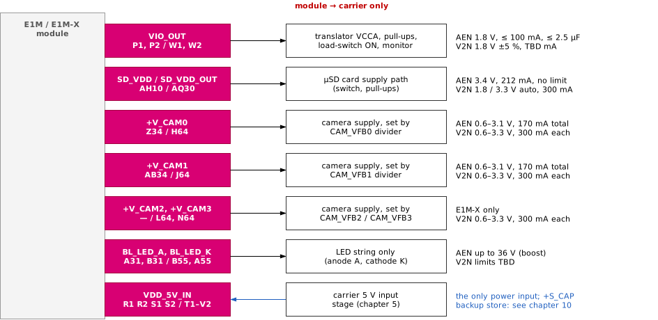
SoM output rails and their pads (E1M / E1M-X): each flows from the SoM to one kind of carrier load; VDD_5V_IN is the only power input; +S_CAP is an RTC backup-store connection that a carrier charger may feed per the SoM manifest (chapter 10)
6.1 The Output-rail Rule
| ID | Level | Rule | Source |
|---|---|---|---|
| CB-RAIL-01 | MUST | Never drive, back-feed or connect another supply to VIO_OUT, SD_VDD / SD_VDD_OUT or +V_CAM0–+V_CAM3. Sourcing current into them fights the on-module regulator and can damage the SoM. | E1M-STD §6.1.2 (2), §6.7.1; HG-V2N-001 |
| CB-RAIL-02 | MUST | Never connect VIO_OUT to another 1.8 V rail, not even one at the same voltage. | E1M-STD §6.1.2 (2); HG-AEN-001 |
| CB-RAIL-03 | MUST | Never use the output-rail pads as GPIO: POWER_* pads have no GPIO secondary function. Do not use them as test inputs either (Guide). | E1M-STD §8.2; Guide (informative) |
| CB-RAIL-04 | SHOULD | Treat each output rail as off until the SoM has switched it on. E1M-AEN switches SD_VDD and +V_CAMx under firmware control and they are off by default; the default state on E1M-X V2N / V2N-M1 is not documented (SD_VDD_OUT switches its voltage between 1.8 V and 3.3 V automatically). | DS-AEN-001, HG-AEN-001; DS-V2N-001 |
6.2 VIO_OUT
VIO_OUT is the SoM's 1.8 V I/O reference (E1M P1, P2; E1M-X W1, W2). It is high while the SoM's I/O domain is powered and low when the SoM is off. Its permitted uses are fixed by E1M-STD §6.1.2 (3):
- (a) the SoM-side supply (VCCA) of carrier level translators, and the pull-up rail for signals into the SoM's 1.8 V pads;
- (b) a module-on indication;
- (c) the enable input of a carrier load switch that makes a carrier 1.8 V rail that follows the SoM.
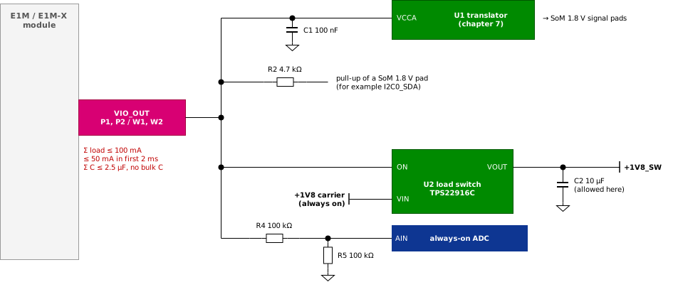
Reference use of VIO_OUT: translator VCCA with its local decoupling, a pull-up, the ON input of load switch U2 (TPS22916C) that switches a carrier 1.8 V rail, and a 100 kΩ / 100 kΩ divider to an always-on ADC
VIO_OUT rules| ID | Level | Rule | Source |
|---|---|---|---|
| CB-RAIL-05 | MUST | Use VIO_OUT only for uses (a), (b) and (c) above. Supply any other carrier load that must follow the SoM from a switched carrier rail (use c). | E1M-STD §6.1.2 (3) |
| CB-RAIL-06 | MUST | Keep the total carrier load on VIO_OUT at or below 100 mA. | E1M-STD §6.1.2 (4) |
| CB-RAIL-07 | MUST | Draw no more than 50 mA from VIO_OUT during the first 2 ms after it rises. Count the inrush of translator VCCA decoupling and of the load-switch ON input. | E1M-STD §6.1.2 (4) (value: E1M-AEN only) |
| CB-RAIL-08 | MUST | Keep the total capacitance on VIO_OUT at or below 2.5 μF, including every decoupling capacitor on translator VCCA pins and pull-up rails. Put bulk capacitance on the switched carrier rail, never on VIO_OUT. | E1M-STD §6.1.2 (4) (value: E1M-AEN only) |
| CB-RAIL-09 | SHOULD | For a carrier 1.8 V rail that follows the SoM, use a load switch whose ON input is driven by VIO_OUT (for example TI TPS22916C or Diodes AP22916), supplied from an always-on carrier 1.8 V rail. | HG-AEN-001 |
| CB-RAIL-10 | MUST | Sense VIO_OUT only through a high-impedance input whose own supply is on whenever the SoM can be powered: a divider into an always-on ADC, or a 1.8 V-tolerant input of an always-on device. Never through a GPIO of a host that can be unpowered. | E1M-STD §6.1.2 (6) |
| CB-RAIL-11 | SHOULD | Sense VIO_OUT itself, not the switched carrier rail; the switched rail lags VIO_OUT and stays up while its output capacitance discharges. | HG-AEN-001 |
| CB-RAIL-12 | SHOULD | Treat VIO_OUT as 1.8 V. Choose translators whose VIO_OUT-side supply (VCCA) is rated 1.65–3.6 V, so the same part keeps working if a later revision defines another level. | E1M-STD §6.1.2 note (informative) |
Bulk capacitance on VIO_OUT above 2.5 μF can stop the SoM's 1.8 V rail from starting.
The 2.5 μF budget fills quickly: one 100 nF capacitor per translator and per pull-up group is the most a typical carrier can afford. The 100 kΩ / 100 kΩ divider in the reference circuit loads VIO_OUT with 9 μA and gives the ADC 0.9 V.
E1M-X pad W1 is VIO_OUT, but E1M pad W1 is PORn: never copy a VIO_OUT or PORn circuit between form factors by pad ID (chapter 8).
VIO_OUT high does not mean that every 1.8 V pad of the SoM is safe to drive. Some pads are on internally switched rails (chapter 7), and PORn must also be high before the carrier drives any pad (chapter 8).
6.3 SD-card Supply
The SoM powers the card itself: SD_VDD (E1M AH10) or SD_VDD_OUT (E1M-X AQ30). Chapter 14 covers the card interface.
| ID | Level | Rule | Source |
|---|---|---|---|
| CB-RAIL-13 | MUST | Connect SD_VDD / SD_VDD_OUT only to the card socket supply path: an optional current-limited switch (CB-RAIL-14), the decoupling and the SD line pull-ups of chapter 14. Never connect a carrier supply or regulator output to it. | E1M-STD §6.7.1 |
| CB-RAIL-14 | SHOULD | Protect the card socket on the carrier (current-limited switch or fuse) where the card can be hot-plugged or shorted: E1M-AEN has no current limit on SD_VDD. | HG-AEN-001 |
| CB-RAIL-15 | MUST | Do not build a carrier that feeds AH10 from the carrier. E1M-AEN hw_rev R2 took the SD supply from the carrier on AH10; from hw_rev R3 AH10 is a 3.4 V SoM output, and a carrier supply on it fights the SoM. | E1M-STD §6.7.1; HG-AEN-001 |
6.4 Camera Supplies
The camera supplies are adjustable LDO outputs: +V_CAM0 (E1M Z34, E1M-X H64), +V_CAM1 (AB34 / J64), and on E1M-X only +V_CAM2 (L64) and +V_CAM3 (N64). Each output voltage is set by a carrier divider on the matching CAM_VFBx pad (E1M Z33, AB33; E1M-X H63, J63, L63, N63). Chapter 15 gives the divider design.
| ID | Level | Rule | Source |
|---|---|---|---|
| CB-RAIL-16 | MUST | Fit the feedback divider on every CAM_VFBx whose +V_CAMx the carrier uses, next to the pad. Without it, firmware that enables the LDO drives the camera with an unregulated output. | Guide (damage); DS-AEN-001, DS-V2N-001 |
| CB-RAIL-17 | SHOULD | For a carrier that targets any SoM, set +V_CAMx at or below 3.1 V (the E1M-AEN maximum), and keep the camera load within the smallest declared limit (E1M-AEN: 170 mA for both rails together and 100 mA per rail at a 3.1 V setting; at low output voltages the LDO derates, for example about 96 mA for one rail at a 1.2 V setting and TA = 75 °C). | DS-AEN-001; Guide (informative) |
| CB-RAIL-18 | MUST | Connect no carrier supply or regulator output to a +V_CAMx net. | E1M-STD §6.7.1 |
| CB-RAIL-23 | SHOULD | Use +V_CAMx for camera supplies, or for other light carrier loads within the per-module limit (DS-AEN-001 allows a general-purpose carrier load). | Guide (informative); DS-AEN-001 |
6.5 Backlight Output
BL_LED_A (E1M A31, E1M-X B55) and BL_LED_K (E1M B31, E1M-X A55) connect an LED string to the on-module backlight driver. Chapter 16 gives the full circuit. On an assembly without the backlight driver (E1M-AEN assembly option; E1M-X V2N / V2N-M1 compound pad B55 BL_LED_A / BL_PWM) the anode pad is instead BL_PWM, a 1.8 V PWM output to a carrier driver input; chapter 16 gives the safe default fit (LED string, BL_PWM path not fitted).
| ID | Level | Rule | Source |
|---|---|---|---|
| CB-RAIL-19 | MUST | Connect only an LED string (anode on BL_LED_A) and its feedback network. Never connect a logic input or another supply. | E1M-STD §6.7.1 |
| CB-RAIL-20 | MUST | Rate every carrier part and the connector on BL_LED_A for at least the maximum boost voltage the SoM manifest declares, and never below 36 V (E1M-AEN). | E1M-STD §6.7.1 (36 V informative); DS-AEN-001 (damage) |
| CB-RAIL-24 | SHOULD | For a carrier that targets any SoM, rate the parts on BL_LED_A for at least 50 V; the E1M-X V2N / V2N-M1 driver limits are TBD and a 10-LED boost can exceed 36 V. | Guide (informative) |
| CB-RAIL-21 | SHOULD | Make the carrier feedback resistor on BL_LED_K an assembly option until the SoM declares where its feedback resistor sits. | Guide (informative) |
BL_LED_A reaches up to 36 V on E1M-AEN; a logic input on this pad is destroyed.
6.6 Output-rail Budget
Every output rail is generated from VDD_5V_IN. Add its load to the 5 V worksheet of chapter 5 as I5V = (Vrail × Irail) / (η × 5 V), with Vrail the SoM's internal source voltage for LDO rails (E1M-AEN camera LDOs run from 3.4 V) and η the SoM conversion efficiency (85 % is used in this guide when the SoM declares none).
| ID | Level | Rule | Source |
|---|---|---|---|
| CB-RAIL-22 | SHOULD | List every carrier load on each output rail, check it against the per-module limits below, and carry the total into the 5 V worksheet. | E1M-STD §6.1.1 (5); Guide (informative) |
6.7 Per-module Differences
| Rail | E1M-AEN | E1M-X V2N | E1M-X V2N-M1 |
|---|---|---|---|
VIO_OUT level | 1.8 V; tolerance TBD | 1.8 V ± 5 % | 1.8 V ± 5 % |
VIO_OUT load | ≤ 100 mA; ≤ 50 mA in the first 2 ms; ≤ 2.5 μF | TBD mA; capacitance TBD; "level translators and small pull-ups only" | TBD mA; capacitance TBD |
| SD-card supply | SD_VDD AH10: 3.4 V fixed, 212 mA, no current limit, off by default | SD_VDD_OUT AQ30: 1.8 V / 3.3 V switched automatically, 300 mA | SD_VDD_OUT AQ30: 1.8 V / 3.3 V switched automatically, 300 mA |
| Camera supplies | +V_CAM0 Z34, +V_CAM1 AB34; 0.6–3.1 V; 170 mA for both together, 100 mA per rail at 3.1 V; off by default | +V_CAM0–+V_CAM3 H64, J64, L64, N64; 0.6–3.3 V; 300 mA each | as E1M-X V2N |
| Camera feedback pin current | 10 nA nominal, 100 nA maximum | not specified | not specified |
| Backlight output | A31 / B31; KTD2801 boost, up to 36 V, input up to 520 mA from VDD; assembly without driver: A31 is BL_PWM, 1.8 V PWM output (DS-AEN-001) | B55 / A55; driver optional (assembly); boost voltage and limits TBD; feedback resistor location not stated; without driver: B55 is BL_PWM, 1.8 V PWM output (DS-V2N-001) | as E1M-X V2N |
| Earlier hardware revisions | hw_rev R2: VIO_OUT 200 mA; SD_VDD a carrier input; +V_CAMx 0.6–3.3 V, 300 mA each | — | — |
6.8 Checklist
| Done | Check | Rule |
|---|---|---|
| ☐ | No carrier supply, regulator output or other rail connected to any SoM output rail | CB-RAIL-01, −02, −13, −18, −23 |
| ☐ | VIO_OUT used only as translator VCCA, pull-up rail, module-on indication or load-switch enable | CB-RAIL-05 |
| ☐ | VIO_OUT load summed: ≤ 100 mA total, ≤ 50 mA in the first 2 ms | CB-RAIL-06, −07 |
| ☐ | VIO_OUT capacitance summed: ≤ 2.5 μF; bulk capacitance only on the switched rail | CB-RAIL-08 |
| ☐ | VIO_OUT sensed through a high-impedance input on an always-on supply | CB-RAIL-10 |
| ☐ | No carrier supply on AH10 (E1M) | CB-RAIL-15 |
| ☐ | Divider fitted on every used CAM_VFBx; camera voltage and load within the limits | CB-RAIL-16, −17 |
| ☐ | BL_LED_A net and connector rated for the declared boost voltage, never below 36 V (50 V for any SoM); only an LED string connected | CB-RAIL-19, −20, −24 |
| ☐ | Output-rail loads carried into the 5 V worksheet | CB-RAIL-22 |
7 I/O Levels, Level Shifting and Back-powering
Almost every signal pad of a conformant SoM is a 1.8 V pad powered from the SoM's VIO_OUT domain. Two things follow for the carrier: carrier logic at another level reaches these pads only through a level translator referenced to VIO_OUT, and nothing on the carrier may push current into a pad while the SoM is off. A pad that receives current while the SoM is unpowered back-powers the SoM through its input clamp: the SoM can start in an undefined state, draw current from the wrong source, or be damaged.
7.1 Pad Voltage Domains
Unless E1M-STD §6.7.1 or the SoM manifest lists it otherwise, every signal pad is in the VIO_OUT (1.8 V) domain. The pads outside that domain are MODULE_EN (up to 5.5 V), VDD_5V_IN, the SoM output rails (chapter 6), SD_CLK / SD_CMD / SD_D0–SD_D3 (SD-card supply levels), BL_LED_A / BL_LED_K, the Ethernet MDI pairs, ANT_*, the USB pads, the CSI / DSI / PCIe pairs, the CAN pads (per the declared CAN option, chapter 18) and +S_CAP.
| ID | Level | Rule | Source |
|---|---|---|---|
| CB-IO-01 | MUST | Treat every signal pad as a VIO_OUT-domain pad unless E1M-STD §6.7.1 or the SoM manifest places it in another domain. | E1M-STD §6.7.1 |
| CB-IO-02 | MUST | Never clamp a pad outside the VIO_OUT domain to VIO_OUT, pull it up to VIO_OUT or level-translate it as a 1.8 V signal. Apply the rule of its own domain. | E1M-STD §6.7.1 |
| CB-IO-03 | MUST | Keep every VIO_OUT-domain pad between −0.3 V and 1.98 V at all times. | E1M-STD §6.2.3 (5) |
| CB-IO-04 | MUST | Of the control pads, only MODULE_EN may be pulled or driven above VIO_OUT. Never drive MODULE_STBY, PORn or JTAG_nRST above VIO_OUT. Fit no carrier pull-up on PORn (CB-CTL-08), and pull JTAG_nRST up, if at all, only to VIO_OUT. Chapter 8 gives the control-pad circuits. | E1M-STD §6.2.3 (2), §6.3.1 (2) to (4) |
| CB-IO-27 | SHOULD | Fit no carrier pull-up on MODULE_STBY, not even to VIO_OUT: the SoM pulls it up internally to a rail that stays on while VIO_OUT is low, and a carrier resistor to VIO_OUT then pulls the pad low (CB-CTL-17). | Guide (informative), stricter than E1M-STD §6.3.1 (2) |
MODULE_STBY is 5 V tolerant only on E1M-AEN hw_rev R3; on E1M-X V2N / V2N-M1 it is pulled up to 1.8 V, and a 3.3 V or 5 V pull-up on it overdrives the pad.
7.2 1.8 V Logic Levels
E1M-STD-1.0 revision 1.4 gives DC characteristics only in the informative tables of §6.6, and for the VIO_OUT-domain signal pads (VIL, VIH, VOL, VOH, drive strength, leakage) they read "per SoM datasheet". Design to the E1M-AEN values below. The input levels VIL / VIH equal 0.35 / 0.65 × 1.8 V (JESD8-7); the output levels are the E1M-AEN datasheet values, not the JESD8-7 ones (0.45 V and VDD − 0.45 V). The input thresholds scale with VIO_OUT: at the E1M-X V2N / V2N-M1 upper tolerance (1.89 V) 0.65 × VDD is about 1.23 V, so a carrier output at exactly 1.17 V has no margin. Drive SoM inputs from logic referenced to VIO_OUT, or with VOH at or above 0.65 × VIO_OUTmax (about 1.23 V).
| Parameter | Min | Max | Carrier design consequence |
|---|---|---|---|
| VOL, SoM output low | — | 0.4 V | Carrier input VIL at or above 0.4 V plus margin |
| VOH, SoM output high | 1.4 V | — | Carrier input VIH at or below 1.4 V minus margin |
| VIL, SoM input low | — | 0.63 V | Carrier output VOL at or below 0.63 V |
| VIH, SoM input high | 1.17 V | — | Carrier output VOH at or above 0.65 × VIO_OUT (1.17 V at 1.8 V, about 1.23 V at 1.89 V) and at or below 1.98 V |
Absolute maximum, any VIO_OUT-domain pad | −0.3 V | 1.98 V | CB-IO-03 |
| ID | Level | Rule | Source |
|---|---|---|---|
| CB-IO-05 | SHOULD | Connect carrier logic directly to a VIO_OUT-domain pad only if it runs from VIO_OUT (or a rail switched by it) and meets the levels above. Everything else goes through a level translator. | DS-AEN-001; Guide (informative) |
7.3 Back-powering
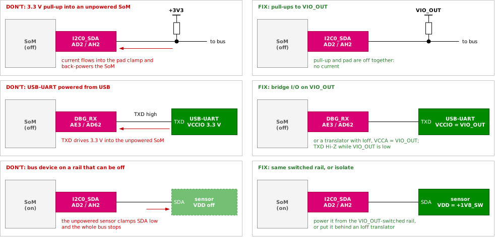
Three common back-power paths and their fixes: a pull-up to an always-on rail, a USB-UART bridge powered from USB, and a bus device on a rail that can be off
| ID | Level | Rule | Source |
|---|---|---|---|
| CB-IO-06 | MUST | While VIO_OUT is low, never drive a VIO_OUT-domain pad high and never source current into it, whether from a push-pull output, a pull-up resistor, a debug probe, a USB-to-UART bridge or any other carrier circuit. Pull-down resistors and open-drain outputs that only pull low are allowed at any time. | E1M-STD §6.2.3 (1) |
| CB-IO-07 | MUST | Pull every VIO_OUT-domain pad up only to VIO_OUT or to a carrier rail switched by VIO_OUT. Never to 3.3 V, 5 V or an always-on 1.8 V rail. This permits a pull-up; it does not require one. MODULE_STBY and PORn get no carrier pull-up at all (CB-IO-04, CB-IO-27). | E1M-STD §6.2.3 (4) |
| CB-IO-08 | MUST | Debug probes and console adapters on the debug pads (DBG_TX / DBG_RX, JTAG / SWD): use VIO_OUT as the target reference, disable the probe's target-power output, and keep the probe outputs high-impedance while VIO_OUT is low. | E1M-STD §6.2.3 (6), §7.3.10, §7.3.13 |
| CB-IO-09 | MUST | Connect a host, USB-to-UART bridge or other device that is powered independently of the SoM to SoM pads only through a translator referenced to VIO_OUT (CB-IO-17, CB-IO-18), or supply its I/O from VIO_OUT. | E1M-STD §6.2.3 (1) |
| CB-IO-10 | SHOULD | Power devices that share a bus with the SoM from the VIO_OUT-switched rail, or choose devices with power-off-protected (Ioff) I/O, or isolate them with a translator. An unpowered device clamps the bus low through its own input clamps. | Guide (informative) |
| CB-IO-11 | SHOULD | Count every carrier pull-up and static load on SoM pads in the standby budget. A 10 kΩ pull-up held low at 1.8 V draws 0.18 mA (calculated); SoM standby currents are in the microampere range. | HG-AEN-001 |
A pull-up from an always-on 3.3 V rail into a VIO_OUT-domain pad back-powers the unpowered SoM through the pad clamp.
7.4 I/O Gating
The carrier drives VIO_OUT-domain pads only while the SoM is powered and out of reset. E1M-STD §6.2.1 orders it: First apply 5 V; Then wait until VIO_OUT is high and PORn is high; Only then drive the pads. On power-down the carrier releases the pads within 1 ms of PORn falling.
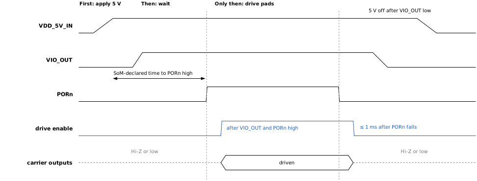
I/O gating: carrier outputs are enabled only after VIO_OUT and PORn are high, and are released within 1 ms after PORn falls
| ID | Level | Rule | Source |
|---|---|---|---|
| CB-IO-12 | MUST | Use VIO_OUT high together with PORn high as the condition for driving any VIO_OUT-domain pad. | E1M-STD §6.2.3 (3), §6.2.1 |
| CB-IO-13 | MUST | When PORn falls, set every output that drives a SoM signal pad to high impedance or low within 1 ms. | E1M-STD §6.2.2 (2) (value: E1M-AEN only) |
| CB-IO-14 | MUST | Where the SoM declares an additional delay after VIO_OUT and PORn are high before it can receive signals, wait for that delay as well. | E1M-STD §6.2.1 |
| CB-IO-15 | SHOULD | Implement the gate in hardware: translator output-enable driven from PORn and powered from VIO_OUT (see the push-pull reference below), or carrier logic supplied from the VIO_OUT-switched rail. Host firmware alone does not cover a host that boots, resets or crashes independently of the SoM. | Guide (informative) |
| CB-IO-16 | SHOULD | Make VIO_OUT the primary gate. Where a SoM does not declare that it pulls PORn low before its I/O rail falls (E1M-X V2N / V2N-M1 document no controlled power-down; E1M-AEN hw_rev R2 has no supervisor), the PORn term alone does not stop drive into a falling VIO_OUT (CB-IO-06); translators referenced to VIO_OUT release the pads when VIO_OUT falls. | Guide (informative); DS-V2N-001 §4.2 |
The E1M-EVK enables its RP2040-to-module translator (TXS0108E) from the power-good of its VIO_OUT-switched rail, so the RP2040 cannot drive an unpowered module.
7.5 Level-translator Selection
| ID | Level | Rule | Source |
|---|---|---|---|
| CB-IO-17 | MUST | Supply the SoM side (VCCA / VREF) of every carrier level translator from VIO_OUT. | E1M-STD §6.1.2 (3) |
| CB-IO-18 | MUST | Use only translators that keep both ports high-impedance while the VIO_OUT-side supply is off (Ioff, partial-power-down or VCC isolation specified in the datasheet). Pass-gate translators that conduct with VCCA at 0 V do not qualify. | E1M-STD §6.1.2 (5) |
| CB-IO-19 | SHOULD | Use fixed-direction translators with tied direction pins for push-pull signals (UART, SPI, GPIO, PWM, encoder). | Guide (informative) |
| CB-IO-20 | SHOULD | Use an open-drain-capable translator for I2C and other open-drain lines: N-FET pass transistors with VGS(th) ≤ 1.0 V and their gates on VIO_OUT, or a TCA9406-class translator with VCCA = VIO_OUT. Fit pull-ups on both sides and keep the total bus capacitance at or below 400 pF (Standard and Fast mode). | Guide (informative); I2C specification |
| CB-IO-21 | SHOULD | Use auto-direction translators only within the datasheet limits for external pull resistors and load capacitance; prefer fixed-direction parts. | Guide (informative) |
| CB-IO-22 | SHOULD | Choose translators whose VCCA is rated 1.65–3.6 V (forward compatibility, CB-RAIL-12). | E1M-STD §6.1.2 note (informative) |
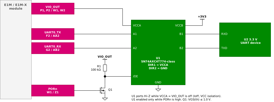
Push-pull translator reference (UART shown): U1 (SN74AXC4T774-class) with VCCA = VIO_OUT and VCCB = 3.3 V; Q1 enables U1 only while PORn is high
In the push-pull reference, R1 holds /OE high (outputs disabled) until Q1 turns on with PORn high. When VIO_OUT falls, U1 releases both ports through its VCC isolation. Q1 adds only its gate capacitance to PORn (limit 1 nF, chapter 8) and is high-impedance with any supply state; R1 loads VIO_OUT with 18 μA while the translator is enabled.
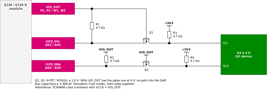
Open-drain translator reference (I2C shown): pull-ups to VIO_OUT on the SoM side, N-FET pass transistors Q1 and Q2 with their gates on VIO_OUT, pull-ups to 3.3 V on the device side
With VIO_OUT low, the gates of Q1 and Q2 are at 0 V and the SoM-side pull-ups have no supply, so no current reaches the SoM pads; the body diodes of Q1 and Q2 are reverse-biased by the 3.3 V side.
7.6 Switched On-module Pad Groups
Some SoMs supply a group of their VIO_OUT-domain pads from an internal rail that can be off while VIO_OUT is high, for example the pads of an on-module radio or coprocessor. For these pads VIO_OUT high is not enough.
| ID | Level | Rule | Source |
|---|---|---|---|
| CB-IO-23 | MUST | For every pad the SoM manifest lists as supplied from an internally switched rail, apply CB-IO-06 while that rail is off, even while VIO_OUT is high. | E1M-STD §6.2.3 (7) |
| CB-IO-24 | SHOULD | Do not fit pull-ups on switched pads; pull-downs are allowed. A pull-up of at least 100 kΩ to VIO_OUT on an E1M-AEN Wi-Fi pad is a documented E1M-AEN exception to CB-IO-23 (it sources a small current while Wi-Fi is off); fit it only in a build that declares an E1M-AEN SoM set, and on other SoMs only where the manifest permits it. | HG-AEN-001, DS-AEN-001 |
| CB-IO-25 | MUST | In the default assembly keep pads that an on-module coprocessor owns (E1M-X V2N-M1: the DX-M1 pads in the table below) high-impedance or input-only. Driving them contends with the coprocessor. | DS-V2N-M1-001; Guide (damage) |
7.7 Pads with Module-specific Uses
E1M-AEN uses GPIO pad IO25 (E1M P3) as RTC_WAKE_N, an open-drain output that its datasheet asks to pull up to an always-on rail of up to 5.5 V. IO25 is a plain 1.8 V GPIO in the standard (absolute maximum 1.98 V), and on E1M-X it is a different pad (F63).
| ID | Level | Rule | Source |
|---|---|---|---|
| CB-IO-26 | MUST | Do not fit a pull-up above VIO_OUT on E1M P3 (IO25) in the default assembly. A pull-up to an always-on rail for the E1M-AEN RTC_WAKE_N function is an assembly option, not fitted by default, used only in a build that declares an E1M-AEN-only SoM set. | E1M-STD §6.2.3 (4), §6.7.2 (1); HG-AEN-001 |
A pull-up from an always-on 3.3 V rail on E1M P3 overdrives the 1.8 V IO25 pad of every E1M SoM other than E1M-AEN.
7.8 Per-module Differences
| Item | E1M-AEN | E1M-X V2N | E1M-X V2N-M1 |
|---|---|---|---|
| 1.8 V logic levels | VOL ≤ 0.4 V, VOH ≥ 1.4 V, VIL ≤ 0.63 V, VIH ≥ 1.17 V | not specified (datasheet rows empty) | not specified (datasheet rows empty) |
| Absolute maximum, 1.8 V pads | −0.3 V to 1.98 V | −0.3 V to 1.98 V | −0.3 V to 1.98 V |
| Pads on an internally switched rail | Wi-Fi module pads IO13 (E3), IO15–IO24 (F3–O3) and SPI1 (AG8, AG9, AG10, AH8, AH9): powered only while Wi-Fi is on | supervisor-MCU (GD32) pads: IO8–IO16 (AR21, AQ21, AR22, AQ22, AR23, AQ23, AR24, AQ24, AR25), IO25–IO32 (F63, F64, AN63, AN64, AO63, AO64, AP63, AP64), IO34 (AQ64), IO35 (A25), PWM0–PWM7, ENC*; power state relative to VIO_OUT TBD | as E1M-X V2N |
| Pads owned by a coprocessor | Wi-Fi pads above | GD32 pads above | as E1M-X V2N, plus DX-M1 pads IO0 L2, IO1 M2, IO2 N2, IO3 O2, IO4 AF2, IO5 AG2, IO6 AL2, IO17 AQ26, IO18 AR26, IO19 AQ27, IO20 AR27, IO21 AQ28, IO22 AR28, IO24 AR29: not carrier GPIO with the stock firmware |
| SD data lines | at SD_VDD (3.4 V) through an on-module translator; valid only while SD_VDD is on | at SD_VDD_OUT (1.8 V / 3.3 V) | at SD_VDD_OUT (1.8 V / 3.3 V) |
MODULE_STBY | 5 V tolerant; about 1 MΩ internal pull-up | pulled up to 1.8 V; not 5 V tolerant | pulled up to 1.8 V; not 5 V tolerant |
PORn | 100 kΩ to 1.8 V and 1 nF on-module; pulled low on every power-off and brownout | pulled up to 1.8 V; behaviour on power-down not documented | as E1M-X V2N; also resets the DX-M1 |
VIO_OUT in low-power states | high in run and STOP; low in self-off and shutdown | TBD in RTC-only standby | TBD in RTC-only standby |
| Ready to receive signals | PORn high, 206 ms typical / 290 ms maximum after VDD reaches 4.75 V or MODULE_EN release | no ready output; hand-off delay TBD | no ready output; hand-off delay TBD |
IO25 (E1M P3 / E1M-X F63) | RTC_WAKE_N, open-drain output (AEN-specific use) | GD32 GPIO (F63) | GD32 GPIO (F63) |
| Earlier hardware revisions | hw_rev R2: MODULE_STBY is an RTC event input, 1.8 V only (100 kΩ pull-up to 1.8 V), not 5 V tolerant; no supervisor, so PORn is not pulled low on brownout | — | — |
7.9 Checklist
| Done | Check | Rule |
|---|---|---|
| ☐ | Every pad classified: VIO_OUT domain or another domain per E1M-STD §6.7.1 and the SoM manifest | CB-IO-01, −02 |
| ☐ | No VIO_OUT-domain pad can see more than 1.98 V or less than −0.3 V | CB-IO-03 |
| ☐ | No carrier pull-up on MODULE_STBY / PORn; JTAG_nRST pulled up only to VIO_OUT; none driven above VIO_OUT | CB-IO-04, −27 |
| ☐ | Every pull-up on a VIO_OUT-domain pad goes to VIO_OUT or the VIO_OUT-switched rail | CB-IO-07 |
| ☐ | No push-pull output, probe, bridge or pull-up can source current into a pad while VIO_OUT is low | CB-IO-06, −08, −09 |
| ☐ | Pad drive gated on VIO_OUT high and PORn high, in hardware where possible | CB-IO-12, −15 |
| ☐ | Carrier outputs released within 1 ms after PORn falls | CB-IO-13 |
| ☐ | All translators: VCCA = VIO_OUT, Ioff or VCC isolation specified | CB-IO-17, −18 |
| ☐ | I2C translators: open-drain capable, pull-ups both sides, ≤ 400 pF | CB-IO-20 |
| ☐ | Switched pad groups of every target SoM handled; no pull-ups on them (E1M-AEN ≥ 100 kΩ exception only in an E1M-AEN build) | CB-IO-23, −24 |
| ☐ | E1M-X V2N-M1 DX-M1 pads high-impedance or input-only by default | CB-IO-25 |
| ☐ | E1M P3 (IO25): no pull-up above VIO_OUT in the default assembly | CB-IO-26 |
| ☐ | Standby budget includes every pull-up and static load on SoM pads | CB-IO-11 |
8 Control Pins, Module States and Power Sequencing
This chapter covers the control pads (MODULE_EN, MODULE_STBY, PORn), the module-specific wake output RTC_WAKE_N, and the order in which a carrier powers the module up and down. The normative rules are E1M-STD-1.0 revision 1.4 §6.2 (power sequencing), §6.3 (reset and module enable) and §6.3.1 (control-pad drive rules). Values marked (E1M-AEN only) in the specification bind every carrier until a later revision states otherwise.
The circuits in this chapter are the same for every module. A carrier built to them powers up any conformant E1M or E1M-X module with nothing connected to the control pads, and can switch it off, reset it and read its state without depending on a particular module.
8.1 Control pad map
| Signal | E1M pad | E1M-X pad | Function (E1M-STD §6.3) |
|---|---|---|---|
MODULE_EN | O1 | AA1 | Input, active-high, SoM-internal pull-up. Low switches the SoM off and holds it off; release switches it on. 5 V tolerant (−0.3 V to 5.5 V). |
MODULE_STBY | O2 | AB1 | Input, active-low, SoM-internal pull-up. Standby request; the protocol (level or pulse) is declared in the SoM manifest. Not 5 V tolerant on every SoM. |
PORn | W1 | Z1 | Open drain, wired-AND, active-low, SoM-internal pull-up to 1.8 V. Low resets the SoM; the SoM can also hold it low while its rails are not valid. |
JTAG_nRST | Z1 | AL1 | Debug reset, open drain. See Chapter 9. |
VIO_OUT | P1, P2 | W1, W2 | 1.8 V SoM output. High = SoM I/O rail up. See Chapter 6. |
RTC_WAKE_N | P3 (IO25) | — | Module-specific use of a GPIO pad (E1M-AEN only): open-drain RTC wake output. Not defined by the specification. |
E1M pad W1 is PORn but E1M-X pad W1 is VIO_OUT, E1M pad Z1 is JTAG_nRST but E1M-X pad Z1 is PORn, and E1M-X pads AA1 / AB1 are E1M PDM_C0 / PDM_C1, so never copy a control circuit from one form factor to the other by pad ID. A PORn reset button or open-drain N-MOSFET copied from E1M pad W1 to E1M-X pad W1 shorts VIO_OUT to GND on every press or assertion.
A SoM SHALL power up and boot with MODULE_EN, MODULE_STBY and PORn all unconnected (E1M-STD §6.3), so none of these pads needs a carrier pull-up.
8.2 Drive rules that suit every module
The rules below follow E1M-STD §6.3.1. They are written so that one circuit works on every module: they combine the 5 V tolerance and very weak pull-up of E1M-AEN with the 1.8 V pull-ups of E1M-X V2N / V2N-M1 on MODULE_STBY and PORn, and with the possibility that a SoM pulls MODULE_EN up as high as VDD_5V_IN (the E1M-X V2N / V2N-M1 documents state 5 V for that pull-up).
| ID | Strength | Rule | Source |
|---|---|---|---|
| CB-CTL-01 | MAY | Leave MODULE_EN, MODULE_STBY and PORn unconnected when the carrier does not use them. | E1M-STD §6.3 |
| CB-CTL-02 | MUST | Pull MODULE_EN low only with an open-drain or open-collector output, a switch or a push-button to GND. Use push-pull drive only in a build variant whose every declared SoM manifest allows it (E1M-AEN allows 1.8 V to 5 V push-pull; the E1M-X V2N / V2N-M1 documents state open drain). | E1M-STD §6.3.1 (1) |
| CB-CTL-03 | MUST NOT | Fit a pull-up on MODULE_EN to a rail that can be off while VDD_5V_IN is present. A pull-up to an unpowered rail acts as a pull-down and switches the SoM off. | E1M-STD §6.3.1 (1) |
| CB-CTL-04 | MUST | Drive MODULE_EN from a host that can be unpowered while the SoM must stay on only through a buffer (N-MOSFET to GND, Figure 27). An unpowered host GPIO clamps the line low through its ESD diodes. | E1M-STD §6.3.1 (1) |
| CB-CTL-05 | MUST | Rate every carrier part on MODULE_EN (buffer transistor, ESD diode, read-back input) for 5.5 V. Specify the FET IDSS at VDS = 5.5 V. | E1M-STD §6.3.1 (1) |
| CB-CTL-06 | MUST | Keep the total carrier leakage on MODULE_EN and on MODULE_STBY at or below 0.1 μA with the driver released, ESD diodes and FET leakage included, over the operating temperature range. | E1M-STD §6.3.1 (1), (2) (E1M-AEN only) |
| CB-CTL-07 | MUST | Pull MODULE_STBY low only with an open-drain output, a switch or a push-button to GND, on every SoM; this pad has no push-pull manifest exception. Fit no pull-up on it to any rail other than VIO_OUT. | E1M-STD §6.3.1 (2) |
| CB-CTL-17 | SHOULD NOT | Fit any pull-up on MODULE_STBY, not even to VIO_OUT; the SoM pulls it up internally. On E1M-AEN the internal pull-up goes to an always-on 1.8 V rail and on E1M-X V2N / V2N-M1 to 1V8 at the GD32 supervisor, while VIO_OUT can be low in a low-power state. A carrier resistor to VIO_OUT then pulls MODULE_STBY low: E1M-AEN wakes as soon as it enters self-off with wake armed, or is held asleep under the level protocol, and the SoM pull-up back-feeds VIO_OUT through the resistor. | Guide (informative), stricter than E1M-STD §6.3.1 (2); DS-AEN-001 Reset and Control; DS-V2N-001 pin list |
| CB-CTL-08 | MUST | Pull PORn low only with an open-drain output, a switch or a push-button to GND. Never drive it high and fit no carrier pull-up. | E1M-STD §6.3.1 (3) |
| CB-CTL-09 | MUST | Hold PORn low for at least 2 ms, and for at least the minimum the SoM manifest declares. | E1M-STD §6.3.1 (3) (E1M-AEN only) |
| CB-CTL-10 | MUST | Add no more than 1 nF on PORn, reset-button capacitor and ESD capacitance included. | E1M-STD §6.3.1 (3) (E1M-AEN only) |
| CB-CTL-11 | MUST | Read PORn only with an input that is specified high-impedance while unpowered (Ioff or partial-power-down), whatever rail supplies it, for example a 74LVC1G34. A plain CMOS input supplied from VIO_OUT does not meet this: while VIO_OUT is low and the SoM holds PORn up, its ESD diode feeds PORn into the unpowered VIO_OUT rail. | E1M-STD §6.3.1 (3) |
| CB-CTL-12 | MUST | Sense VIO_OUT only through a high-impedance input whose own supply is on whenever the SoM can be powered. A GPIO of a host that can be unpowered does not meet this: put an Ioff buffer between them that is supplied from the host rail and accepts a 1.8 V input (for example SN74LV1T34), with a pull-down of 100 kΩ or more at its input so that the level is defined while VIO_OUT is off. | E1M-STD §6.1.2 (6) |
| CB-CTL-13 | SHOULD | Make PORn and MODULE_EN reachable on every carrier, by a button or at least a test pad, for recovery. | HG-V2N-001 design checklist; HG-AEN-001 Reference Carrier Configurations |
| CB-CTL-14 | SHOULD | Fit a button on MODULE_EN, MODULE_STBY or PORn with no debounce capacitor and only a low-leakage ESD diode (the module filters the line; firmware debounces). | HG-AEN-001 Control Pins |
| CB-CTL-15 | SHOULD NOT | Use MODULE_EN low as the normal power-off path. It is a hard power cut. | E1M-STD §6.3.1 (1) |
| CB-CTL-16 | MUST | In a generic variant treat P3 as IO25, a 1.8 V VIO_OUT-domain GPIO: fit a pull-up only to VIO_OUT or to a rail switched by VIO_OUT. A pull-up of RTC_WAKE_N to an always-on rail (≤ 5.5 V, ≥ 10 kΩ) is permitted only in a variant declared for E1M-AEN hw_rev R3 or later, and it is conformant only when the E1M-AEN manifest declares P3 outside the VIO_OUT domain (E1M-STD §6.7.1, §6.2.3 (2)). E1M-STD-1.0 revision 1.4 does not yet contain that declaration (see the specification notes at the end of this chapter). | E1M-STD §6.2.3 (2), (4), §6.7.1, §8.4; DS-AEN-001 pin list, R2 → R3 changes |
A pull-up from P3 to an always-on 3.3 V rail drives a 1.8 V GPIO pad above its 1.98 V absolute maximum on any E1M module other than E1M-AEN.
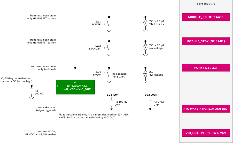
Carrier reference circuit for the control pads: buttons to GND with low-leakage ESD, PORn read-back and I/O-enable buffer, RTC_WAKE_N options (not fitted)
In Figure 26, U1 is a single buffer with Ioff (for example a 74LVC1G34) supplied from VIO_OUT, with PORn as its input. Its output IO_EN is high only while VIO_OUT is high and PORn is high; the 100 kΩ pull-down R1 holds it low while U1 is unpowered. IO_EN is active high (high = enabled): connect it directly only to translators with an active-high output enable (Chapter 7). Many direction-controlled translators have an active-low /OE (for example SN74LVC8T245, SN74AXC8T245, SN74AVC4T245); wired straight to IO_EN, they are enabled exactly while the SoM is off or in reset. For those, invert IO_EN with an Ioff inverter and fit a pull-up on /OE to the supply that the translator data sheet references the OE input to, so that /OE reads "disabled" while U1 or the inverter is unpowered. This implements the I/O gate of E1M-STD §6.2.3 (3) in hardware, and it gives a host a PORn read-back that cannot load PORn while the host is off.
The EVK's debug controller can hold PORn low but cannot read it back, so no procedure on that board can wait for PORn in hardware; only VIO_OUT is observable. Provide a PORn read-back as in Figure 26.
8.2.1 N-MOSFET buffer for a host that can be unpowered
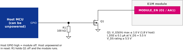
MODULE_EN driven through an N-MOSFET from a host that can be unpowered
- Host GPIO high = SoM off. While the host is unpowered or in reset, the 100 kΩ gate pull-down keeps
Q1off and the SoM runs. - Choose
Q1with VGS(th) max well below the host VOH (≤ 1.0 V for a 1.8 V host), a VDS rating ≥ 5.5 V and IDSS ≤ 0.1 μA at VDS = 5.5 V over the operating temperature range. The E1M EVK uses Diodes DMN31D5UFZ-7B; check its IDSS at 5.5 V and at the carrier's maximum temperature before reuse. - The 100 kΩ gate pull-down draws 18 μA from a 1.8 V GPIO while it holds the SoM off; count it in a battery budget.
- Use the same circuit on
MODULE_STBY(host GPIO high = standby request).
8.2.2 PORn
- Reset button to
GND, no capacitor, or ≤ 1 nF (CB-CTL-10). A 100 nF capacitor, common on reset buttons, slows the reset release from about 0.1 ms to about 10 ms on E1M-AEN and delays the reset on a 5 V loss (HG-AEN-001). PORnlow stops the SoC with no notice to firmware; a non-volatile write in progress is lost or corrupted. Use it for recovery, not as a normal reset path.- On E1M-X V2N-M1,
PORnalso resets the on-module DX-M1; the module boot firmware releases the DX-M1 afterwards.
8.2.3 MODULE_STBY
- Button to
GNDor an open-drain host output (N-MOSFET buffer). No carrier pull-up at all (CB-CTL-17), no debounce capacitor, low-leakage ESD only. - The standby protocol is module and firmware specific and is declared in the SoM manifest (E1M-STD §6.3.1 (2)). Do not design carrier logic that depends on one module's protocol unless the variant is declared for that module.
8.2.4 RTC_WAKE_N (E1M-AEN only)
E1M-AEN uses P3 (IO25) as an open-drain, active-low RTC wake output that stays low until firmware clears the RTC flags. It is valid in every power state while 5 V is present. The specification does not define this function; it is a tertiary function under E1M-STD §8.4, so a carrier that relies on it declares an E1M-AEN dependency.
- Generic variant: leave
P3asIO25. If the carrier reads it, fit ≥ 100 kΩ toVIO_OUTor to a rail switched byVIO_OUT(R2in Figure 26). The signal is then visible only while the SoM is on. - Variant declared for E1M-AEN (hw_rev R3 or later): to wake a carrier host or PMIC while the module is in self-off, pull it up to an always-on rail ≤ 5.5 V with ≥ 10 kΩ (
R3, for example 1 MΩ for the standby budget) and use an edge-triggered host wake input, because the pad can stay low indefinitely.
8.3 Power-up sequence
The SoM sequences all of its own rails (E1M-STD §6.2). The carrier orders only the control pads and the signal pads:
- First, apply
VDD_5V_INwithin the limits of Chapter 5. To keep the SoM off, holdMODULE_ENlow before and whileVDD_5V_INrises; otherwise leaveMODULE_ENreleased. - Then wait until
VIO_OUTis high andPORnis high, and then for any additional hand-off delay the SoM manifest declares. - Only then drive the signal pads of the SoM. Until then keep every carrier output that connects to the SoM high-impedance or low.
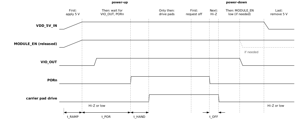
Generic power-up and power-down sequence. Parameter values per module are in the per-module differences table of this chapter
8.4 Power-down sequence
- First, request a graceful shut-down by the means the SoM manifest declares (application link, a GPIO, or
MODULE_STBY), and give firmware time to finish its writes. A host timeout of 2 s before the fallback is a sensible value for E1M-AEN (HG-AEN-001). - Next, when
PORnfalls, set every output that drives a SoM signal pad to high impedance or low within 1 ms. Remove the drive also whenVIO_OUTfalls, whichever comes first. - Then, if the SoM has not powered off by itself, force it off with
MODULE_ENlow. - Last, remove
VDD_5V_IN, preferably afterVIO_OUTis low.
Pulling MODULE_EN low, pulling PORn low or removing VDD_5V_IN gives the SoM firmware no notice, so a write to on-module non-volatile memory in progress at that moment is lost or corrupted.
| ID | Strength | Rule | Source |
|---|---|---|---|
| CB-SEQ-01 | MUST | Follow the power-up order: 5 V first; then wait for VIO_OUT high and PORn high; only then drive SoM signal pads. | E1M-STD §6.2.1 |
| CB-SEQ-02 | MUST | Hold MODULE_EN low before and while VDD_5V_IN rises when the SoM must stay off at power-up. | E1M-STD §6.2.1 (1) |
| CB-SEQ-03 | MUST | Wait for the additional hand-off delay the SoM manifest declares after VIO_OUT and PORn are high. A hardware gate on VIO_OUT and PORn alone does not cover it. A carrier with a host adds the delay in host firmware. A carrier without a host (configurations A and B) delays IO_EN in hardware, for example with a reset supervisor supplied from VIO_OUT that senses PORn through a high-impedance input and has a capacitor-programmed delay, sized when the SoM declares tHAND. | E1M-STD §6.2.1 |
| CB-SEQ-04 | MUST | Use VIO_OUT high together with PORn high as the condition for driving VIO_OUT-domain signal pads. | E1M-STD §6.2.3 (3) |
| CB-SEQ-05 | MUST | Set every output that drives a SoM signal pad to high impedance or low within 1 ms after PORn falls. | E1M-STD §6.2.2 (2) (E1M-AEN only) |
| CB-SEQ-06 | MUST | Drive no VIO_OUT-domain pad high and source no current into it while VIO_OUT is low, whatever PORn does. Translators supplied from VIO_OUT on their SoM side do this by themselves only when they are specified Ioff / partial-power-down on both ports (E1M-STD §6.1.2 (5)); pass-gate translators are excluded, because some conduct with VCCA at 0 V. | E1M-STD §6.2.3 (1), §6.1.2 (5) |
| CB-SEQ-07 | SHOULD | Implement the gate of CB-SEQ-04 in hardware (IO_EN in Figure 26), not only in host firmware. | Guide (informative) |
| CB-SEQ-08 | SHOULD | Request a graceful shut-down before any forced power-off. | E1M-STD §6.2.2 (1) |
| CB-SEQ-09 | SHOULD | Remove VDD_5V_IN only after VIO_OUT is low. | E1M-STD §6.2.2 (4) |
| CB-SEQ-10 | SHOULD | For a forced power cycle hold MODULE_EN low for ≥ 25 ms; a carrier that cycles VDD_5V_IN instead keeps it off for ≥ 1 s for a guaranteed restart (E1M-AEN, not yet characterised). | HG-AEN-001 Power Sequences, Reference Carrier Configurations |
8.5 Reference carrier configurations
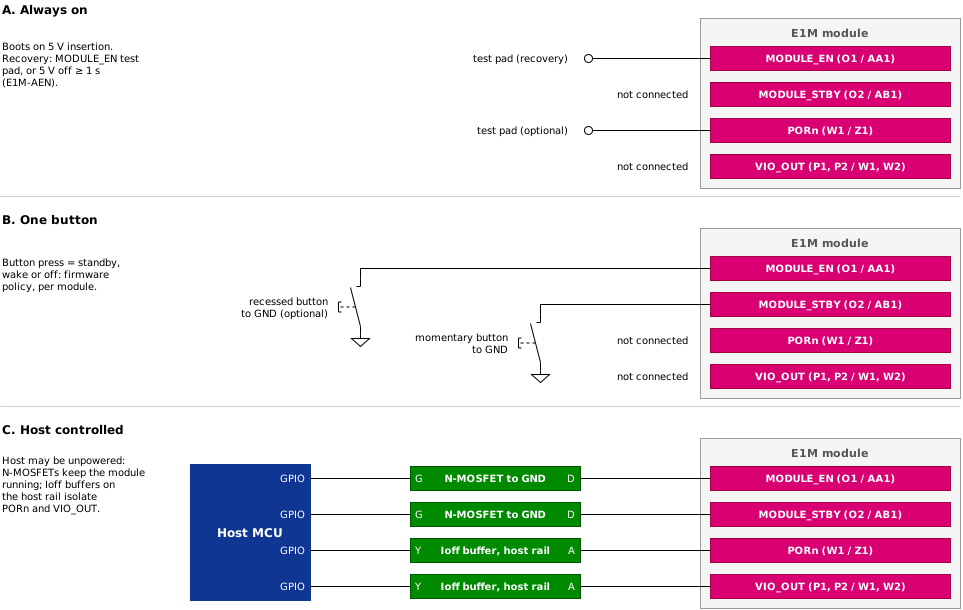
Reference carrier configurations A (always on), B (one button) and C (host controlled)
| Configuration | MODULE_EN | MODULE_STBY | Notes |
|---|---|---|---|
| A. Always on | Not connected; test pad for recovery. | Not connected. | Boots on 5 V insertion. On E1M-AEN, firmware that switches the module off without arming a wake leaves it off until 5 V is cycled (≥ 1 s off) or MODULE_EN is pulsed: keep the test pad. |
| B. One button | Not connected, or a recessed button to GND (hard power cut). | Momentary button to GND. | Press behaviour (standby, wake, off) is firmware policy and module specific. No pull-up, no debounce capacitor; low-leakage ESD only. |
| C. Host controlled | Host through an N-MOSFET to GND (Figure 27). | Host through an N-MOSFET to GND. | Host reads VIO_OUT and PORn through Ioff buffers that are supplied from the host rail and accept a 1.8 V input (for example SN74LV1T34), not through plain GPIOs: an unpowered host GPIO clamps PORn and is back-powered from VIO_OUT (CB-CTL-11, −12). Push-pull drive of MODULE_EN from 1.8 V to 5 V logic is an E1M-AEN-only option (CB-CTL-02); MODULE_STBY is open drain on every SoM (CB-CTL-07). |
8.6 Module states and timing
The carrier sees the module state only on VIO_OUT and PORn. On E1M-AEN, run and STOP look the same on these pads (both high); a carrier that needs to tell them apart uses an application signal. Whether VIO_OUT stays high during the E1M-X V2N / V2N-M1 RTC-only standby is not documented, so a generic carrier gates its I/O on VIO_OUT and PORn in every state and does not assume which pads stay powered in standby.
| Item | E1M-AEN | E1M-X V2N | E1M-X V2N-M1 |
|---|---|---|---|
MODULE_EN pad | O1. 5 V tolerant (5.5 V max). Clamp FET into an always-on 1.8 V rail, about 1 MΩ internal pull-up to that rail. Released, the carrier side of the pad floats to about 1.2–1.5 V; module input threshold 1.25 V (both HG-AEN-001; see the specification notes); 1.0 ms filter. Open drain preferred; push-pull 1.8 V to 5 V allowed (VOH 1.45–5.5 V, VOL ≤ 0.4 V at 3.3 μA). | AA1. Open drain. Internal pull-up to "VDD" (pin list), "VDDIN" (DS-V2N-001 §6), "5 V" (HG-V2N-001); thresholds not stated. | AA1. As E1M-X V2N; low shuts down both RZ/V2N and DX-M1. |
MODULE_EN timing | Low pulse < 0.5 ms ignored; low ≥ 2 ms always off; ≥ 25 ms full power cycle (DS-AEN-001 also states about 21 ms); high ≥ 2 ms after a low always boots. | TBD. | TBD. |
MODULE_STBY pad | O2. Active low, 5 V tolerant, same circuit as MODULE_EN (about 1 MΩ internal pull-up to an always-on 1.8 V rail). Pulse protocol (≥ 2 ms low, ≥ 2 ms high between pulses) or level protocol (firmware). Wake from self-off: low ≥ 10 ms, armed by firmware. | AB1. Open drain, pull-up to 1V8. Request to the GD32 supervisor; reference firmware enters RTC-only standby. Timing TBD. | AB1. As E1M-X V2N; the DX-M1 enters its lowest-power retention state. |
PORn pad | W1. 100 kΩ pull-up to 1.8 V and 1 nF on the module. Released about 2 ms after the module 1.8 V rail is up. On-module supervisor holds it low below 1.65 V (hw_rev R3). Carrier pulse ≥ 2 ms. | Z1. Pull-up to 1V8. Minimum low pulse "TBD μs". | Z1. As E1M-X V2N; also resets the DX-M1. |
VDD_5V_IN ≥ 4.75 V or MODULE_EN release to PORn high (tPOR) | 206 ms typ, 290 ms max. | TBD; no ready output. | TBD; DX-M1 powered later by boot firmware. |
| Additional hand-off delay (tHAND) | None declared. | TBD (fixed delay after MODULE_EN release, DS-V2N-001 §4.2). | TBD. |
Outputs Hi-Z after PORn falls (tOFF) | ≤ 1 ms. | Not stated; PORn behaviour at power-down not documented. | Not stated. |
| 5 V ramp (tRAMP) | Monotonic, 0 V to 4.75 V within 40 ms. | Not specified. | Not specified. |
| Graceful power-off | Application link, IO8 / IO10, or long MODULE_STBY press (firmware policy); module self-off. | Not documented; DS-V2N-001: MODULE_EN low, then remove 5 V. | As E1M-X V2N. |
RTC_WAKE_N | P3 (IO25), open drain, ≤ 5.5 V. | None. | None. |
| hw_rev scope | Every E1M-AEN-only option in this chapter (5 V tolerant or push-pull MODULE_STBY, RTC_WAKE_N) needs hw_rev R3 or later. On R2, MODULE_STBY is a 1.8 V input with 100 kΩ to 1.8 V (not 5 V tolerant) and P3 is not connected (DS-AEN-001 R2 → R3 changes). | — | — |
| Low-power currents | Shutdown 2.94 μA, self-off 1.14 μA, STOP 3.84 μA (typical, calculated, not measured on hw_rev R3). | Sleep and shutdown TBD. | TBD. |
E1M-X V2N / V2N-M1 do not document whether PORn falls before their I/O rail at power-down, so the 1 ms rule after PORn falls cannot be checked on those modules. A carrier whose translators are supplied from VIO_OUT and enabled by IO_EN stops driving on whichever signal falls first.
8.7 Specification notes
- Annex A.1 states that E1M-AEN
MODULE_STBY"enters real-time-clock standby only". DS-AEN-001 (hw_rev R3) describes sleep / STOP, wake and self-off control on that pad; this guide uses the DS-AEN-001 behaviour. - §6.3.1 (2) permits a pull-up from
MODULE_STBYtoVIO_OUT. That pull-up breaks module states on E1M-AEN and E1M-X V2N / V2N-M1 (CB-CTL-17); the clause should forbid any carrier pull-up. - No manifest clause or Annex A.1 entry declares E1M-AEN
P3(RTC_WAKE_N) outside theVIO_OUTdomain, so the always-on pull-up of CB-CTL-16 is not yet conformant. The E1M-AEN manifest should declareP3as open drain, up to 5.5 V (§6.7.1). - HG-AEN-001 gives a released
MODULE_ENlevel of about 1.2–1.5 V and a module input threshold of 1.25 V. The guide reads the first as the carrier side of the on-module clamp FET and the second as the internal node; confirm both against the hw_rev R3 netlist.
8.8 Chapter checklist
| Check | Rule | |
|---|---|---|
| ☐ | No carrier pull-up on MODULE_EN, MODULE_STBY or PORn. | CB-CTL-03, −08, −17 |
| ☐ | MODULE_EN, MODULE_STBY and PORn are driven only by open drain, switch or button to GND. | CB-CTL-02, −07, −08 |
| ☐ | A host that can be unpowered drives MODULE_EN / MODULE_STBY through an N-MOSFET with VDS ≥ 5.5 V and IDSS ≤ 0.1 μA at 5.5 V. | CB-CTL-04, −05 |
| ☐ | Every part on MODULE_EN is rated for 5.5 V; released leakage on MODULE_EN and MODULE_STBY ≤ 0.1 μA. | CB-CTL-05, −06 |
| ☐ | PORn: no capacitor or ≤ 1 nF; reset pulse ≥ 2 ms; read-back input specified Ioff / partial-power-down, whatever its supply. | CB-CTL-09, −10, −11 |
| ☐ | VIO_OUT and PORn reach a host that can be unpowered only through Ioff buffers on the host rail. | CB-CTL-11, −12 |
| ☐ | IO_EN polarity matches the translator enable (active-high OE, or inverter plus pull-up on /OE); a hostless carrier delays IO_EN by tHAND. | CB-SEQ-03, −07 |
| ☐ | PORn and MODULE_EN reachable by button or test pad. | CB-CTL-13 |
| ☐ | P3 has no pull-up to an always-on rail unless the variant is declared for E1M-AEN. | CB-CTL-16 |
| ☐ | Carrier drive gated on VIO_OUT high and PORn high, in hardware; host adds the declared hand-off delay. | CB-SEQ-03, −04, −07 |
| ☐ | Carrier outputs go Hi-Z or low within 1 ms after PORn falls, and whenever VIO_OUT is low. | CB-SEQ-05, −06 |
| ☐ | Power-off path requests a graceful shut-down first; MODULE_EN low only as fallback. | CB-SEQ-08, CB-CTL-15 |
| ☐ | Control circuits drawn from the pad table of the board's own form factor (no copied pad IDs). | Pad map warning |
9 Boot Configuration and Debug Access
This chapter covers the four boot-strap pads, the JTAG / SWD debug pads and the debug console UART. The normative sources are E1M-STD-1.0 revision 1.4 §6.4 (boot configuration), §6.2.3 (back-powering, including debug probes), §6.3.1 (4) (JTAG_nRST), §7.3.10 (debug UART), §7.3.13 (SWD / JTAG) and §8.3 (compound-function pads). All of these pads are in the VIO_OUT (1.8 V) domain.
9.1 Boot straps
| Signal | E1M pad | E1M-X pad | Function |
|---|---|---|---|
BOOT0 | V2 | Y2 | Boot strap bit 0. Interpretation declared in the SoM manifest. |
BOOT1 | U2 | X2 | Boot strap bit 1. |
BOOT2 | U1 | X1 | Boot strap bit 2. Drive per the manifest default or leave to the SoM's internal pull. |
BOOT3 | V1 | Y1 | Boot strap bit 3. |
Every conformant SoM has BOOT0–BOOT3 on its footprint at these pads (E1M-STD §6.4 (1)). The meaning of the strap is silicon specific and is declared in the SoM manifest (§6.4 (2)). A SoM whose boot does not depend on the strap may ignore the four pads, and then declares in its manifest that it ignores them (§6.4 (3)); E1M-AEN does this and is conformant. The carrier keeps its strap circuit for every module: on a module that ignores the strap the circuit has no effect (§6.4 (4)). On the reference E1M-X modules the RZ/V2N samples all four pads at the rising edge of PORn, so the strap levels must be stable before PORn rises; the carrier changes them only while the SoM is held in reset or off.
E1M strap pads U1, U2, V1 and V2 are VDD_5V_IN pads on E1M-X, so a strap circuit placed by pad ID on an E1M-X footprint connects 5 V to VIO_OUT through the switch and destroys the module.
Strap and debug pads also swap between the form factors:
| Pad ID | E1M | E1M-X |
|---|---|---|
X1 | JTAG_TCK/SWDCLK | BOOT2 |
X2 | JTAG_TDI | BOOT1 |
Y1 | JTAG_TMS/SWDIO | BOOT3 |
Y2 | JTAG_TDO | BOOT0 |
Z1 | JTAG_nRST | PORn |
U1, U2, V1, V2 | BOOT2, BOOT1, BOOT3, BOOT0 | VDD_5V_IN |
A debug header placed by E1M pad ID on an E1M-X footprint drives the E1M-X boot straps and resets the SoM through PORn; an E1M-X strap switch or pull-up network placed on an E1M footprint ties the JTAG / SWD pads to VIO_OUT or GND.
9.1.1 Strap circuit for any module
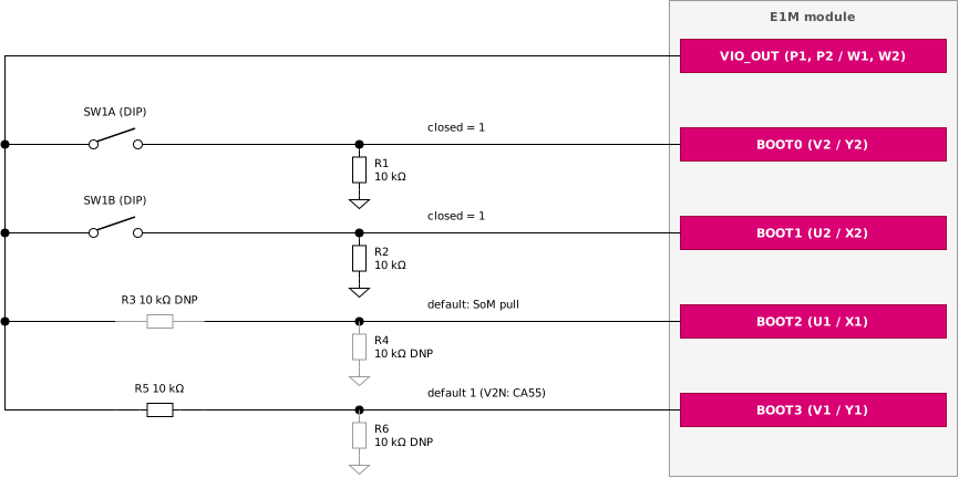
Boot-strap circuit for any module: DIP switch to VIO_OUT with 10 kΩ pull-downs on BOOT0 / BOOT1, BOOT3 pulled up, BOOT2 options not fitted
BOOT0,BOOT1: a 2-position DIP switch toVIO_OUTwith 10 kΩ pull-downs (R1,R2). Switch closed = 1. A production carrier may replace the switch by fixed resistors.BOOT2: no resistor fitted by default, so the SoM's internal pull or manifest default applies.R3/R4(10 kΩ, not fitted) allow a fixed level if a SoM manifest asks for one.BOOT3: 10 kΩ pull-upR5toVIO_OUTfitted (1 = CA55 boot on the reference E1M-X modules), pull-downR6not fitted. The E1M-X V2N documents do not state an internal default pull onBOOT3, so the carrier sets the level.- On E1M-AEN the four strap pads are not connected on the module and the manifest declares the strap ignored (E1M-STD §6.4 (3)); the circuit has no effect there and the carrier needs no separate variant for it.
- Each closed switch draws 180 μA from
VIO_OUTthrough its 10 kΩ pull-down; count it in theVIO_OUTload (Chapter 6).
BOOT1 | BOOT0 | Boot mode | Device | CA55 boot | CM33 boot |
|---|---|---|---|---|---|
| 0 | 0 | Mode 0 | eSD (3.3 V) | Supported | Not supported |
| 0 | 1 | Mode 1 | eMMC (1.8 V I/O) | Supported | Not supported |
| 1 | 0 | Mode 2 | QSPI NOR (1.8 V I/O) | Supported | Supported |
| 1 | 1 | Mode 3 | SCIF download | Supported | Supported |
| ID | Strength | Rule | Source |
|---|---|---|---|
| CB-BOOT-01 | MUST | Drive BOOT2 according to the SoM manifest's declared default, or leave it to the SoM's internal pull. | E1M-STD §6.4 |
| CB-BOOT-02 | MUST | Pull strap pads up only to VIO_OUT or to a rail switched by VIO_OUT, never to an always-on rail. | E1M-STD §6.2.3 (4) |
| CB-BOOT-03 | MUST | If a host drives the strap pads (for example through 10 kΩ series resistors from GPIOs), keep its outputs high-impedance or low while VIO_OUT is low. | E1M-STD §6.2.3 (1) |
| CB-BOOT-04 | SHOULD | Provide a means to set BOOT0 and BOOT1: a 2-position DIP switch to VIO_OUT with 10 kΩ pull-downs, or fixed straps on a production carrier. | HG-V2N-001 Boot; DS-V2N-001 §5 |
| CB-BOOT-05 | SHOULD | Fit a 10 kΩ pull-up from BOOT3 to VIO_OUT, with a not-fitted pull-down option, rather than relying on an internal pull. | Guide (informative) |
| CB-BOOT-06 | MUST | Draw the strap circuit from the pad table of the board's own form factor; never reuse E1M pad IDs on an E1M-X footprint (5 V on U1, U2, V1, V2 destroys the module). | E1M-STD §7.3.1 pad tables; guide derivation (damage) |
| CB-BOOT-07 | SHOULD | Hold strap levels stable while PORn rises; change a DIP switch only with the SoM in reset or off. | DS-V2N-001 §5 |
| CB-BOOT-08 | MUST | Draw the debug header from the pad table of the board's own form factor: on E1M-X, pads X1, X2, Y1, Y2 are the boot straps and Z1 is PORn; on E1M they are the JTAG / SWD pads and JTAG_nRST. | E1M-STD §7.3.1, §7.3.13 pad tables; guide derivation |
On E1M-X V2N-M1 the Alp Lab-supplied U-Boot alone enables the 0.75 V DX-M1 core rail and releases the DX-M1 in a fixed order, and a replacement boot loader or any second writer to the on-module PMIC can bring that rail up at the PMIC's 1.80 V default and damage the DX-M1 (HG-V2N-M1-001 Boot).
Flashing stock DEEPX firmware to the DX-M1 leaves its NPUs dead (dxrt_polling_ack: timeout), and recovery needs a boot-strap change on the module that is not a field operation (DS-V2N-M1-001; HG-V2N-M1-001; rule CB-BRU-11 in Chapter 23).
9.2 JTAG / SWD debug
| Signal | E1M pad | E1M-X pad | Notes |
|---|---|---|---|
JTAG_TCK/SWDCLK | X1 | AJ1 | Compound pad: JTAG clock or SWD clock. |
JTAG_TMS/SWDIO | Y1 | AK1 | Compound pad: JTAG mode select or SWD data. |
JTAG_TDI | X2 | AJ2 | JTAG only. |
JTAG_TDO | Y2 | AK2 | JTAG only. |
JTAG_nRST | Z1 | AL1 | Debug reset from the probe, open drain. |
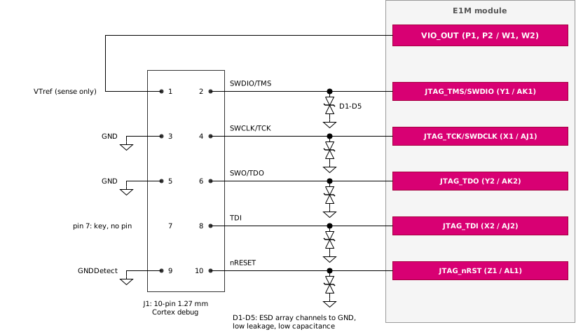
10-pin 1.27 mm Cortex debug header: pin-out and module pads, VTref from VIO_OUT
| Header pin | Probe signal | Carrier connection |
|---|---|---|
| 1 | VTref | VIO_OUT (E1M P1, P2 / E1M-X W1, W2), sense only |
| 2 | SWDIO / TMS | JTAG_TMS/SWDIO (Y1 / AK1) |
| 3, 5 | GND | GND |
| 4 | SWCLK / TCK | JTAG_TCK/SWDCLK (X1 / AJ1) |
| 6 | SWO / TDO | JTAG_TDO (Y2 / AK2) |
| 7 | key | No pin |
| 8 | TDI | JTAG_TDI (X2 / AJ2) |
| 9 | GNDDetect | GND |
| 10 | nRESET | JTAG_nRST (Z1 / AL1) |
| ID | Strength | Rule | Source |
|---|---|---|---|
| CB-DBG-01 | SHOULD | Expose the JTAG / SWD pads on a 10-pin 1.27 mm Cortex debug header (for example Samtec FTSH-105 series) with VTref connected to VIO_OUT. | HG-AEN-001 JTAG / SWD Debug; DS-V2N-001 §7 |
| CB-DBG-02 | MUST | Use a probe or adapter that takes VIO_OUT as its target reference, has its target-power output disabled, and keeps its outputs high-impedance while VIO_OUT is low. | E1M-STD §6.2.3 (6) |
| CB-DBG-03 | MAY | Select either function of the compound pads (JTAG or SWD). JTAG_TDI and JTAG_TDO are used only in JTAG mode. | E1M-STD §8.3, §7.3.13 |
| CB-DBG-04 | MUST | Pull JTAG_nRST low only with an open-drain output; fit no pull-up on it to any rail other than VIO_OUT. | E1M-STD §6.3.1 (4) |
| CB-DBG-05 | MUST | Connect a 3.3 V probe only through a translator supplied from VIO_OUT on the SoM side, with both ports high-impedance while that supply is off. Keep every debug pad between −0.3 V and 1.98 V. | E1M-STD §6.1.2 (5), §6.2.3 (5) |
| CB-DBG-06 | SHOULD | Fit low-leakage, low-capacitance ESD protection on a debug header that the user can reach from outside the product. | Guide (informative) |
| CB-DBG-07 | MUST NOT | Connect a debug header, probe or programming circuit to any RSVD pad (for example the E1M-AEN Wi-Fi debug pads Q3, R3, T3, S3 or the programming port U3, V3). | E1M-STD §7.3.3 |
| CB-DBG-08 | SHOULD | Bring DBG_TX / DBG_RX to a header or to a USB-to-UART bridge referenced to VIO_OUT. | E1M-STD §7.3.10 |
| CB-DBG-09 | MUST | Drive DBG_RX only while VIO_OUT is high. A USB-to-UART bridge that stays powered from USB while the SoM is off connects through a translator with Ioff on both ports. | E1M-STD §7.3.10, §6.2.3 (1), §6.1.2 (5) |
| CB-DBG-10 | SHOULD | Count the debug path (pull-ups, translator leakage, an unpowered bridge loading the SoM pull-up on DBG_RX) in the standby budget, or isolate it. | HG-AEN-001 JTAG / SWD Debug |
The EVK connects its RP2040 controller (I2C1) to the E1M-AEN RSVD pads U3 / V3 (RSVD5 / RSVD6) through the level shifter U14, and has an RSVD pad header J26 that is not fitted on this build (UG-E1M-001). That is specific to an E1M-AEN development board; a carrier for any module leaves every RSVD pad unconnected (CB-DBG-07).
9.3 Debug console UART
E1M-STD-1.0 revision 1.4 assigns a dedicated debug-console UART in both form factors: DBG_TX (SoM output) and DBG_RX (SoM input), both in the VIO_OUT domain (E1M-STD §7.3.10). Earlier revisions listed these pads as RSVD.
| Signal | E1M pad | E1M-X pad | Direction |
|---|---|---|---|
DBG_TX | AD3 | AC62 | SoM output |
DBG_RX | AE3 | AD62 | SoM input; drive only while VIO_OUT is high |
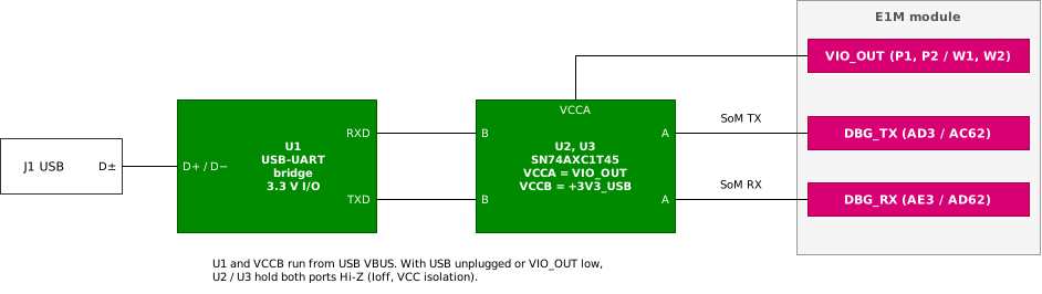
Debug console: bus-powered USB-to-UART bridge with 3.3 V I/O, isolated from the 1.8 V pads by translators supplied from VIO_OUT
U1is any bus-powered USB-to-UART bridge with 3.3 V I/O. It stays powered from USB VBUS while the SoM is off.U2,U3are single-bit direction-controlled translators with Ioff and VCC isolation on both ports (for example TI SN74AXC1T45, VCCA rated 0.65 V to 3.6 V, which also covers the 1.65–3.6 V VCCA range recommended in E1M-STD §6.1.2 for forward compatibility). VCCA =VIO_OUT, VCCB = the bridge 3.3 V rail. Tie eachDIRpin for its fixed direction.- With USB unplugged or
VIO_OUTlow, both ports ofU2/U3are high-impedance: the bridge cannot back-power the SoM, and the SoM cannot back-power the bridge. - A carrier that has no room for a bridge brings the two pads,
VIO_OUTandGNDto a 4-pin header for an external 1.8 V adapter (CB-DBG-02 applies to the adapter).
On E1M-AEN, DBG_TX / DBG_RX are the Alif Secure Enclave UART, also used to program MRAM with the Alif Security Toolkit. Code that programs MRAM keeps every erase range below 0x80578000: the Secure Enclave boot table occupies 0x80578000–0x8057FFFF, and erasing it can leave the module unbootable (HG-AEN-001 JTAG / SWD Debug).
9.4 Per-module differences
| Item | E1M-AEN | E1M-X V2N | E1M-X V2N-M1 |
|---|---|---|---|
BOOT0–BOOT3 | Not connected on the module (no boot-strap pins; boot from MRAM); strap declared ignored in the manifest (E1M-STD §6.4 (3)). | (BOOT1, BOOT0): 00 eSD (3.3 V), 01 eMMC, 10 QSPI NOR, 11 SCIF download. Sampled at the PORn rising edge. | As E1M-X V2N; the DX-M1 is not affected by the straps. |
BOOT2 | Not connected. | DS-V2N-001 Boot Settings and Boot Modes: "fixed at 1"; DS-V2N-001 pin list: "Not connected. Leave floating." | As E1M-X V2N. |
BOOT3 | Not connected. | High = CA55 boot, low = CM33 boot; internal default pull not stated. | As E1M-X V2N. |
JTAG_nRST | Z1. "Active-low system reset request from the debug probe" (DS-AEN-001), 20 kΩ pull-up to 1.8 V on the module. | AL1. "Active-low reset to the SoC debug logic" (DS-V2N-001 §7), a debug-logic reset, not a system reset; module pull not stated. | AL1. As E1M-X V2N. |
| JTAG / SWD target | Alif Ensemble SoC, 1.8 V. | RZ/V2N, 1.8 V. | RZ/V2N, 1.8 V. |
| Debug UART | AD3 / AE3: Secure Enclave UART (SE-UART); 33 Ω series on TX, 1 kΩ series and 1 MΩ pull-up to 1.8 V on RX, on the module. Console settings not stated. | AC62 / AD62: on-module debug UART. HG-V2N-001 bring-up uses a console at 115 200 8N1; the pads carrying it are not stated. | As E1M-X V2N. |
| Boot-loader hazard | Keep MRAM erases below 0x80578000. | — | Replacement U-Boot must run the full DX-M1 rail, reset and multiplexer sequence; no stock DEEPX firmware on the DX-M1. |
9.5 Chapter checklist
| Check | Rule | |
|---|---|---|
| ☐ | Strap circuit drawn from the board's own form-factor pad table; no strap part on an E1M-X 5 V pad. | CB-BOOT-06 |
| ☐ | Debug header drawn from the board's own form-factor pad table; no E1M JTAG circuit on E1M-X X1, X2, Y1, Y2, Z1, no E1M-X strap circuit on E1M JTAG pads. | CB-BOOT-08 |
| ☐ | BOOT0 / BOOT1 settable (DIP to VIO_OUT with 10 kΩ pull-downs, or fixed straps). | CB-BOOT-04 |
| ☐ | BOOT2 left to the SoM pull by default; BOOT3 pulled up to VIO_OUT. | CB-BOOT-01, −05 |
| ☐ | No strap pull-up to an always-on rail; host-driven straps Hi-Z while VIO_OUT is low. | CB-BOOT-02, −03 |
| ☐ | 10-pin Cortex header with VTref = VIO_OUT; probe target power off. | CB-DBG-01, −02 |
| ☐ | JTAG_nRST open drain only; no pull-up other than to VIO_OUT. | CB-DBG-04 |
| ☐ | 3.3 V probes or bridges only through VIO_OUT-referenced translators with Ioff. | CB-DBG-05, −09 |
| ☐ | ESD on a user-reachable debug header. | CB-DBG-06 |
| ☐ | No RSVD pad connected to any debug or programming circuit. | CB-DBG-07 |
| ☐ | DBG_TX / DBG_RX brought to a header or a VIO_OUT-referenced USB-to-UART bridge. | CB-DBG-08 |
10 RTC Backup Store (+S_CAP)
The module's real-time clock keeps time from the 5 V input whenever VDD_5V_IN is present. To keep time while 5 V is removed, the carrier connects a backup store to +S_CAP. E1M-STD-1.0 revision 1.4 puts +S_CAP outside the VIO_OUT domain and leaves its electrical behaviour to the SoM manifest (E1M-STD §6.7.1). The module documents differ a lot here, so this chapter separates what is safe on every module from what is safe only on E1M-AEN.
10.1 Pads
| Signal | E1M pad | E1M-X pad | Function |
|---|---|---|---|
+S_CAP | AG15 | AQ25 | RTC backup store connection. Domain and limits as declared in the SoM manifest (E1M-STD §6.7.1). |
RTC_CLKOUT | AH16 | AQ16 | 32 kHz RTC clock output. On E1M-AEN a 1.8 V output, valid only while VIO_OUT is high: treat it as a VIO_OUT-domain output, not as an always-on clock. |
10.2 Backup store options
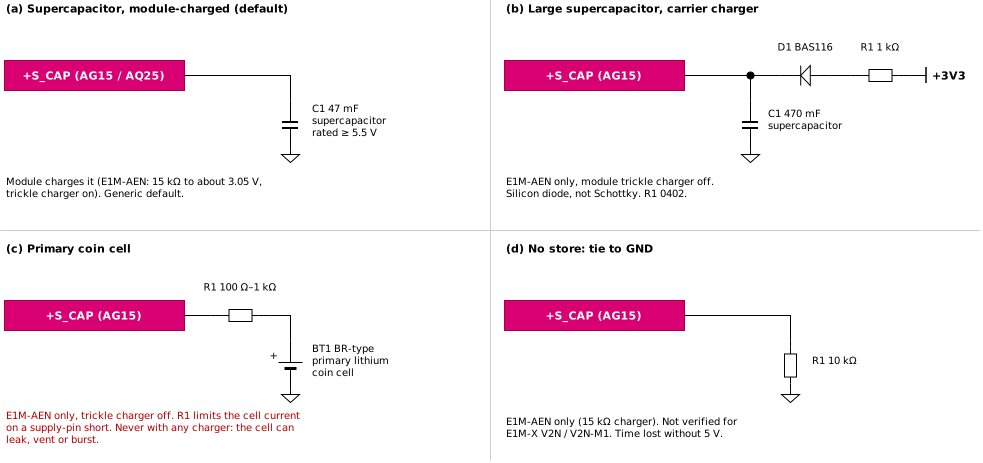
Backup store options on +S_CAP: (a) module-charged supercapacitor, (b) large supercapacitor with carrier charger, (c) primary coin cell, (d) tie to GND
| Option | Carrier circuit | Module setting | Where it is safe |
|---|---|---|---|
| (a) Supercapacitor, module-charged | Supercapacitor from +S_CAP to GND, nothing else. E1M-AEN charges it through 15 kΩ from its always-on 3.3 V rail to about 3.05 V; use it up to about 100 mF. | E1M-AEN: RTC trickle charger enabled, 15 kΩ (never a lower value). | Every module whose documents name a supercapacitor on +S_CAP (E1M-AEN; E1M-X V2N / V2N-M1: "external super-capacitor connection"). Generic default. |
| (b) Large supercapacitor, carrier charger | Supercapacitor, plus 1 kΩ 0402 from a carrier 3.3 V rail that is up whenever the carrier has 5 V, then a low-leakage silicon switching diode (for example BAS116, anode on the resistor, cathode on +S_CAP). Not a Schottky diode. | E1M-AEN: RTC trickle charger disabled, so the two chargers never work at the same time. | Only in a variant declared for E1M-AEN. |
| (c) Primary coin cell | BR-type primary lithium cell rated −40 °C to +85 °C, with a 100 Ω–1 kΩ series resistor between the cell and +S_CAP; the resistor limits the cell current if a solder fault shorts the supply pins. No charger of any kind. | E1M-AEN: RTC trickle charger disabled. | Only in a variant declared for E1M-AEN. |
| (d) No store | +S_CAP tied to GND through 10 kΩ (RTC manufacturer recommendation, DS-AEN-001); never left floating. Time is lost when 5 V is removed. | E1M-AEN: trickle charger disabled. | Only in a variant declared for E1M-AEN. Not verified for E1M-X V2N / V2N-M1, whose charger is not documented. |
A primary lithium cell on +S_CAP that is charged by the module trickle charger or by a carrier charger can leak, vent or burst.
On E1M-AEN +S_CAP must never float, so a carrier must not use a jumper or store-select header whose open position leaves the pad unconnected.
On the EVK, opening jumper P16 leaves +S_CAP floating because the 0 Ω tie to GND (R223) is not fitted. A product carrier fits the store directly, without a jumper.
10.2.1 Generic carrier recommendation
- Fit option (a): one supercapacitor from
+S_CAPtoGND, no jumper and no charger. 47 mF is a practical size. - Rate it at ≥ 5.5 V, the
+S_CAPabsolute maximum of E1M-AEN, until the charge voltage of E1M-X V2N / V2N-M1 is documented. A part rated ≥ 3.3 V is enough in a variant declared for E1M-AEN only. - A supercapacitor rated ≥ 5.5 V is usually two cells in series, often with balancing; its self-discharge or leakage current can be in the μA range, far above the RTC load. Choose a low-leakage part and take its leakage at the charge voltage and temperature from the data sheet into the hold-time calculation (Sizing).
- Provide footprints for options (b), (c) and (d) only in build variants that declare E1M-AEN, and document the matching firmware setting for each variant.
- Do not offer a coin-cell option on a generic carrier until every supported module documents a charger that is off and cannot be enabled while a primary cell is fitted.
10.3 Sizing
The store keeps the RTC running until it falls to the RTC switch-over threshold. On E1M-AEN that threshold is 2.0 V typical, 2.2 V worst case, well above the RTC's own 1.1 V minimum. The hold time of a supercapacitor C charged to VCHG with an RTC load IRTC is about
thold ≈ C (VCHG − VTH) / (IRTC + Ileak)
where Ileak is the self-discharge or leakage current of the store plus the carrier leakage on +S_CAP.
With the E1M-AEN values (VCHG = 3.05 V, VTH = 2.0 V, IRTC about 125 nA at 25 °C) and no store leakage, this gives about 2.3 h per mF: 47 mF keeps time for about 4.6 days at 25 °C (3.7 days worst case). These are upper limits: a store leakage of 1 μA alone shortens the 47 mF hold time to about 12 h. The hold time is much shorter at high temperature, because the RTC current and the capacitor leakage rise.
Through the module's 15 kΩ charger the time constant with 47 mF is about 12 min: an empty store reaches 2.0 V in about 13 min. Leave a new carrier powered for at least 15 min, with firmware that enables the trickle charger, before testing timekeeping without 5 V. Use the carrier charger (option (b)) for stores larger than about 100 mF or when the backup must be ready within minutes: 470 mF then reaches 2.0 V in about 9 min and keeps time for about 30–40 days at 25 °C (E1M-AEN).
10.3.1 Carrier charger (option (b), E1M-AEN only)
With the carrier 3.3 V rail V3V3, the diode forward voltage VF and the store at Vstore, the charge current and the float voltage are
Ichg = (V3V3 − VF − Vstore) / R, Vfloat ≈ V3V3 − VF
Choose R ≥ (V3V3 − VF − Vstore,min) / Imax, where Imax is the maximum charge current of the store. Then check that Vfloat stays below the store rating and below 5.5 V (the E1M-AEN +S_CAP absolute maximum), and above 2.2 V so that the RTC runs from the store, and that the resistor power Ichg2 R with an empty store suits its package.
10.4 Leakage and layout
- Keep the total carrier leakage on
+S_CAP(ESD diode, holder, charger diode, board contamination) at or below 10 nA (E1M-AEN). The store's own self-discharge is separate and sets the hold time. - Keep the
+S_CAPtrace short and away from switching nodes. Do not run it under an inductor or next to a switch node. - Rate the store and every part on
+S_CAPfor the product's temperature range, within the module's own range (E1M-AEN: −40 °C to +75 °C). Standard supercapacitors are room-temperature parts; the RTC keeps time without 5 V only over the range of the element fitted. - The store stays charged after the carrier is switched off. Discharge it before handling or probing the board.
10.5 Rules
| ID | Strength | Rule | Source |
|---|---|---|---|
| CB-RTC-01 | MUST NOT | Leave +S_CAP floating, including through an open jumper or store-select position. | HG-AEN-001 RTC Backup; DS-AEN-001 pin list |
| CB-RTC-02 | MUST | Connect to +S_CAP only a backup store and its charger, as the SoM manifest declares; never a logic signal or another supply rail. | E1M-STD §6.7.1 |
| CB-RTC-03 | MUST NOT | Fit a carrier charger, or enable the module trickle charger, while a primary lithium cell is fitted. | HG-AEN-001 RTC Backup (safety) |
| CB-RTC-04 | MUST | Fit a coin cell (with its 100 Ω–1 kΩ series resistor), a carrier charger or a 10 kΩ tie to GND only in a build variant declared for E1M-AEN. The +S_CAP behaviour is what the SoM manifest declares, and E1M-X V2N / V2N-M1 declare no charger, so the safe default is the plain supercapacitor; a primary cell charged by an undeclared charger can burst. | E1M-STD §6.7.1 (+S_CAP as declared in the manifest), §6.7.2 (1) (safe default fit) |
| CB-RTC-05 | SHOULD | In a generic variant fit a low-leakage supercapacitor directly from +S_CAP to GND, rated ≥ 5.5 V, and include its self-discharge in the hold-time calculation. | Guide (informative) |
| CB-RTC-06 | MUST | With a carrier charger fitted, disable the module trickle charger; use a low-leakage silicon diode (not a Schottky) and a resistor from a carrier 3.3 V rail that is up whenever 5 V is present. | HG-AEN-001 RTC Backup |
| CB-RTC-07 | MUST | Never configure the E1M-AEN module charger below 15 kΩ: it drops the RTC supply and puts the RTC's I2C pins above their supply. | HG-AEN-001 RTC Backup |
| CB-RTC-08 | MUST | Keep the float voltage of a carrier charger below 5.5 V and below the store rating, and above 2.2 V. | DS-AEN-001 Absolute Maximum Ratings; UG-E1M-001 RTC charger sizing |
| CB-RTC-09 | SHOULD | Keep the total carrier leakage on +S_CAP at or below 10 nA. | HG-AEN-001; DS-AEN-001 |
| CB-RTC-10 | SHOULD | Document, for every build variant, the store fitted and the firmware charger setting that matches it. | HG-AEN-001 RTC Backup |
| CB-RTC-11 | SHOULD | Rate the store and the parts on +S_CAP for the product temperature range within the module range. | HG-AEN-001; DS-AEN-001 |
| CB-RTC-12 | SHOULD | Treat RTC_CLKOUT as a VIO_OUT-domain output: load it only with inputs that are high-impedance while unpowered, and do not rely on it while VIO_OUT is low. | DS-AEN-001 pin list; E1M-STD §6.2.3 |
10.6 Per-module differences
| Item | E1M-AEN | E1M-X V2N | E1M-X V2N-M1 |
|---|---|---|---|
+S_CAP pad | AG15: RTC backup input of the RV-3028; must not float. hw_rev R3 or later (not on R2). | AQ25: "external super-capacitor connection". | AQ25: as E1M-X V2N. |
| Module charger | 15 kΩ from the always-on 3.3 V rail to about 3.05 V, enabled by firmware (supercapacitor only). | Not documented. | Not documented. |
| Switch-over threshold | 2.0 V typical, 2.2 V maximum. | Not documented. | Not documented. |
Absolute maximum on +S_CAP | 5.5 V. | Not documented. | Not documented. |
| Carrier leakage limit | ≤ 10 nA. | Not documented. | Not documented. |
| On-module store | None in the standard build; room-temperature option (−20 °C to +60 °C) on request. | Not documented; DS-V2N-001 lists only "RTC". | Not documented; DS-V2N-M1-001 calls the RTC "battery-backed". |
Coin cell, carrier charger, tie to GND | Supported (charger setting per option). | Not verified. | Not verified. |
RTC_CLKOUT | AH16, 1.8 V, valid only while VIO_OUT is high. | AQ16, 32 kHz; validity in standby not stated. | AQ16, as E1M-X V2N. |
10.7 Chapter checklist
| Check | Rule | |
|---|---|---|
| ☐ | +S_CAP cannot float in any assembly or jumper position. | CB-RTC-01 |
| ☐ | Generic variant: one supercapacitor, rated ≥ 5.5 V, directly on +S_CAP; no charger, no coin cell. | CB-RTC-04, −05 |
| ☐ | Coin cell (with series resistor), carrier charger and 10 kΩ to GND only in an E1M-AEN-declared variant. | CB-RTC-04 |
| ☐ | No primary cell together with any charger; firmware charger setting documented per variant. | CB-RTC-03, −10 |
| ☐ | Carrier charger: silicon diode (not Schottky), module charger disabled, float voltage 2.2–5.5 V and within the store rating. | CB-RTC-06, −08 |
| ☐ | Leakage on +S_CAP ≤ 10 nA; short trace away from switching nodes. | CB-RTC-09 |
| ☐ | Store rated for the product temperature range. | CB-RTC-11 |
| ☐ | RTC_CLKOUT used only while VIO_OUT is high. | CB-RTC-12 |
11 Ethernet
Every conformant SoM has its Ethernet PHYs on the module. The carrier adds only what sits between the PHY and the cable: magnetics, the RJ-45, ESD protection and, if wanted, link LEDs. This chapter gives one circuit that works with every module in both form factors.
11.1 Contract between SoM and carrier
- The SoM integrates one on-module PHY per exposed Ethernet group and brings out the PHY-side (pre-magnetics) MDI pairs (E1M-STD §6.5, §7.3.6). It declares the highest link rate of each port in its manifest (§7.3.6 (3)).
- The carrier provides the magnetics (discrete or inside the RJ-45), the connector and the MDI ESD protection. It never adds a PHY.
- Each
ETHxgroup has four pairs,DAtoDD, the set 1000BASE-T needs. A 100BASE-TX SoM usesDAandDBonly and may leaveDCandDDunconnected (§7.3.6 (3)).
P, N)| Signal | E1M pads | E1M-X pads |
|---|---|---|
ETH0_DA_P, ETH0_DA_N | AG30, AH30 | AQ59, AR59 |
ETH0_DB_P, ETH0_DB_N | AG29, AH29 | AQ58, AR58 |
ETH0_DC_P, ETH0_DC_N | AG28, AH28 | AQ57, AR57 |
ETH0_DD_P, ETH0_DD_N | AG27, AH27 | AQ56, AR56 |
ETH0_LED0, ETH0_LED1 | AG31, AH31 | AQ60, AR60 |
ETH1_DA_P, ETH1_DA_N | AG23, AH23 | AQ52, AR52 |
ETH1_DB_P, ETH1_DB_N | AG22, AH22 | AQ51, AR51 |
ETH1_DC_P, ETH1_DC_N | AG21, AH21 | AQ50, AR50 |
ETH1_DD_P, ETH1_DD_N | AG20, AH20 | AQ49, AR49 |
ETH1_LED0, ETH1_LED1 | AG24, AH24 | AQ53, AR53 |
On E1M-X the pair order runs from DD at row 56 to DA at row 59 (ETH1: row 49 to row 52). E1M-STD 1.3 and later correct the pad table of earlier spec drafts, which listed the order reversed. Take the pads from the table above or from pinout/x-v1.json. A carrier wired to the old order puts DA and DB on the wrong RJ-45 pins, and 10/100 fallback then fails.
| ID | Rule | Strength | Source |
|---|---|---|---|
| CB-ETH-01 | Provide a magnetic transformer, or a transformer-integrated RJ-45, for every Ethernet port the carrier uses. | MUST | E1M-STD §6.5, §7.3.6 |
| CB-ETH-02 | Do not add an external Ethernet PHY between the SoM and the magnetics. | MUST NOT | E1M-STD §6.5, §7.3.6 |
| CB-ETH-03 | Route all four pairs (DA to DD) of every port the carrier uses, and use magnetics rated for 1000BASE-T, even where the intended SoM is 100BASE-TX only. | MUST | E1M-STD §7.3.6 (3) |
| CB-ETH-04 | Do not route any other net through Ethernet pads that one SoM leaves unconnected (for example DC, DD and all of ETH1 on E1M-AEN). Another SoM drives them. | MUST NOT | E1M-STD §7.3.4 |
11.2 Universal circuit
Figure 34 is the reference circuit for one port. It uses an RJ-45 with integrated 1000BASE-T magnetics, so the same parts serve the 1 Gbit E1M-X modules and the 100 Mbit E1M-AEN. ETH1 is the same circuit on its own pads.
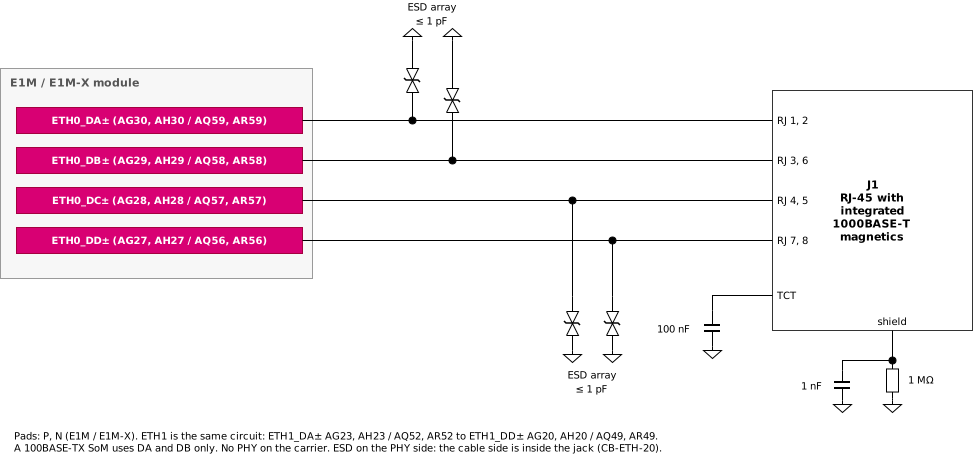
Ethernet port reference circuit with an integrated-magnetics RJ-45: four MDI pairs, PHY-side ESD (CB-ETH-20), centre tap and shield
The RJ-45 pin assignment follows TIA-568: DA on pins 1, 2; DB on 3, 6; DC on 4, 5; DD on 7, 8. E1M-AEN has Auto-MDI/MDIX enabled by default (DS-AEN-001 Ethernet), so a crossed cable also works. The E1M-X V2N and V2N-M1 documents state only that auto-negotiation is enabled by default (HG-V2N-001 Ethernet Interfaces); they do not state Auto-MDI/MDIX. Do not rely on crossover detection for a carrier that hosts any module.
11.3 Magnetics, centre taps and termination
The reference PHYs are TI DP83825 (E1M-AEN) and Realtek RTL8211FI-VD-CG (E1M-X V2N, V2N-M1). Neither module document states the PHY line-driver type or the PHY-side centre-tap connection. Take both from the PHY vendor documents for the PHY that the SoM manifest names: for the reference modules, the TI DP83825I datasheet and reference schematic, and the Realtek RTL8211F(I) / RTL8211FD(I) datasheet and reference schematic. The E1M-EVK 2641-R3 ties the jack's PHY-side centre tap TRCT1 directly to 0 V, with no capacitor (UG-E1M-001 Ethernet).
Figure 35 shows the parts an integrated-magnetics jack contains, drawn for one pair with discrete magnetics.
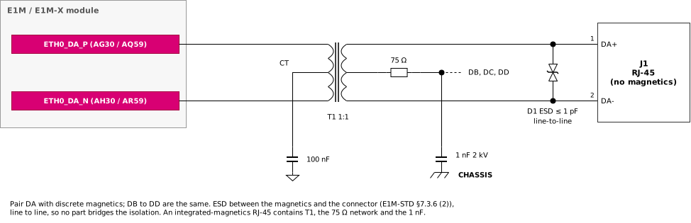
One MDI pair with discrete magnetics: PHY-side ESD, centre-tap capacitor and Bob-Smith termination
| ID | Rule | Strength | Source |
|---|---|---|---|
| CB-ETH-05 | Do not connect a PHY-side centre tap to a supply rail unless the SoM manifest asks for it. A PHY whose line driver needs no centre-tap bias then carries a DC current in its outputs. | SHOULD NOT | Guide (informative); TI DP83825I and Realtek RTL8211F(I) datasheets and reference schematics |
| CB-ETH-21 | Connect each PHY-side centre tap to GND, through 100 nF or directly, as the PHY vendor's reference schematic shows (E1M-EVK 2641-R3: TRCT1 directly to 0 V). | SHOULD | Guide (informative); UG-E1M-001 Ethernet |
| CB-ETH-06 | Terminate each line-side centre tap with 75 Ω to a common node, and that node to chassis through 1 nF rated 2 kV (Bob-Smith termination), or use a jack that contains this network. | SHOULD | Guide (informative) |
| CB-ETH-07 | Connect the RJ-45 shield to chassis or GND through 1 nF in parallel with 1 MΩ (E1M-EVK 2641-R3 precedent). | SHOULD | Guide (informative); UG-E1M-001 Ethernet |
| CB-ETH-08 | Keep copper planes out from under the line side of the magnetics and the jack, except chassis ground, so the isolation barrier is not bridged by a plane. | SHOULD | Guide (informative) |
The EVK precedents differ: HG-AEN-001 names the Abracon ARJM11C7-502-KB-EW2 (a 10/100 jack), and the E1M-EVK 2641-R3 uses HR851178A with four transformer pairs. For a carrier that hosts any module, CB-ETH-03 requires a 1000BASE-T jack. Check the jack datasheet for its centre-tap pins and its internal termination.
11.4 ESD protection
E1M-STD-1.0 revision 1.4 makes MDI ESD a carrier duty for every port that reaches a connector, and names the position: "a low-capacitance ESD array between the magnetics and the connector, with a common-mode choke where needed" (§7.3.6 (2)). HG-AEN-001 (Ethernet Interface) and HG-V2N-001 (Ethernet Interfaces) give the same position. The SoM may also have its own protection, and declares it. On E1M-AEN the DP83825 MDI pins (TD±, RD±) are rated ± 5 kV HBM (ANSI/ESDA/JEDEC JS-001) and its other pins ± 1.5 kV HBM (DS-AEN-001 Ethernet). These are component handling ratings, not IEC 61000-4-2 system ratings: the carrier adds the magnetics, the connector and the IEC 61000-4-2 ESD protection. E1M-X V2N and V2N-M1 have no on-module MDI protection (DS-V2N-001 Ethernet).
| ID | Rule | Strength | Source |
|---|---|---|---|
| CB-ETH-09 | Fit a low-capacitance ESD array on the MDI lines of every port the carrier brings to a connector. | MUST | E1M-STD §7.3.6 (2) |
| CB-ETH-10 | With discrete magnetics, place the ESD array between the magnetics and the connector, connected line to line (Figure 35). Use ≤ 1 pF per line. | MUST | E1M-STD §7.3.6 (2); HG-AEN-001 Ethernet Interface; HG-V2N-001 Ethernet Interfaces |
| CB-ETH-11 | Do not connect a line-to-ground ESD part on the cable side of the magnetics unless it is rated for the isolation test voltage: it bridges the isolation barrier. Line-to-line parts on the cable side are allowed. | SHOULD NOT | Guide (informative); IEEE 802.3 isolation |
| CB-ETH-20 | With an integrated-magnetics RJ-45 the cable side is inside the jack. Place the ESD array on the PHY side, next to the jack, line to GND (Figure 34; E1M-EVK 2641-R3 precedent). Use ≤ 1 pF per line and a working voltage above the MDI swing; E1M-AEN rates its MDI pins − 0.3 V to +4 V. This position differs from the wording of §7.3.6 (2); see the note below. | SHOULD | Guide (informative); UG-E1M-001 Ethernet; DS-AEN-001 Absolute Maximum Ratings |
| CB-ETH-12 | Fit a common-mode choke footprint only where EMC testing shows a need; most integrated-magnetics jacks already contain one. | MAY | E1M-STD §7.3.6 (2) |
Specification conflict. E1M-STD-1.0 revision 1.4 §7.3.6 (2) places the carrier MDI ESD array "between the magnetics and the connector". With an integrated-magnetics RJ-45 that position is inside the jack, so CB-ETH-20 places the array on the PHY side, as the E1M-EVK 2641-R3 does. A reviewer who reads §7.3.6 (2) literally will mark that carrier non-conformant. This guide asks for §7.3.6 (2) to permit PHY-side placement when the magnetics are integrated in the jack (Annex C, C-31). Until the specification changes, declare the ESD position in the carrier build documentation.
11.5 LED pads
ETHx_LED0 and ETHx_LED1 can be PHY configuration straps that the PHY samples at reset. On E1M-AEN they are DP83825 bootstrap pins (DS-AEN-001 Ethernet), with the functions auto-negotiation disable and RX_DV enable (HG-AEN-001 Ethernet Interface). The LED function, polarity and strap role of the E1M-X V2N and V2N-M1 LED pads are not documented. A carrier circuit that loads these pads can therefore mis-strap one module while it works with another.
A pull-up or pull-down on an ETHx_LEDy pad can change the PHY strap at reset, for example disabling auto-negotiation, so the link fails.
The safe circuit puts a translator between the pad and the LED (Figure 36). The translator input draws only leakage, so it does not change the strap level, and its VIO_OUT-side supply keeps it high-impedance while the SoM is off (E1M-STD §6.1.2 (3a), (5)).
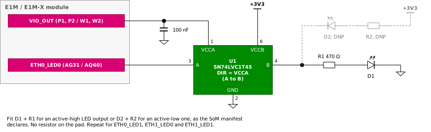
Buffered Ethernet LED drive: SN74LVC1T45 referenced to VIO_OUT, LED position fitted per the declared polarity
| ID | Rule | Strength | Source |
|---|---|---|---|
| CB-ETH-13 | Do not add a pull-up or pull-down resistor to an ETHx_LEDy pad beyond what the SoM manifest allows, and connect LEDs only as the manifest declares. | MUST NOT | E1M-STD §7.3.6 (4) |
| CB-ETH-14 | Drive the LEDs through a translator whose pad-side supply is VIO_OUT (for example SN74LVC1T45, VCCA 1.65–5.5 V, DIR tied to VCCA). Fit the LED position (active-high or active-low) that matches the declared polarity. | SHOULD | Guide (informative); E1M-STD §6.1.2 (3), (5) |
| CB-ETH-15 | A carrier that has no LED circuit leaves the LED pads unconnected. This is safe for every SoM. | MAY | Guide (informative) |
The LED pad is undriven while the PHY is unpowered and VIO_OUT is high. On E1M-AEN the PHY is a switched island that stays off until firmware enables it (DS-AEN-001 Power Architecture). A plain CMOS input such as the SN74LVC1T45 A input has no bus-hold, so it can float in that state: the LED glimmers and the translator draws extra supply current. Use one of these: a translator or buffer with bus-hold or a Schmitt-trigger input on the pad side, after checking that a bus-hold current cannot override the strap at reset; or a high-value pull towards the strap default level, only where the SoM manifest permits it (CB-ETH-13).
The E1M-EVK 2641-R3 drives each LED from an N-MOSFET whose gate is on the LED pad with a 10 kΩ gate pull-down to 0 V (UG-E1M-001 Link LEDs). That pull-down sits on a strap pin. It suits the DP83825 strap defaults, but a generic carrier needs the SoM manifest to allow it (CB-ETH-13).
11.6 Routing
| ID | Rule | Strength | Source |
|---|---|---|---|
| CB-ETH-16 | Route each MDI pair as a 100 Ω differential pair, ± 10 %. | MUST | E1M-STD §7.3.6 (1); HG-AEN-001 Controlled-Impedance Routing |
| CB-ETH-17 | Match the two lines of each pair to ≤ ± 2 ps. | SHOULD | HG-AEN-001; HG-V2N-001 Ethernet Interfaces |
| CB-ETH-18 | Keep the four pairs of one port at similar lengths. No module states an inter-pair limit (HG-V2N-001: TBD). | SHOULD | Guide (informative) |
| CB-ETH-19 | Route the pairs over a solid reference plane, with no other signals between the pairs of one port, and keep them short from the pads to the jack. | SHOULD | Guide (informative) |
11.7 Per-module differences
| Item | E1M-AEN | E1M-X V2N | E1M-X V2N-M1 |
|---|---|---|---|
| PHY | one TI DP83825 on RMII, MDIO address 0 | two Realtek RTL8211FI-VD-CG | as V2N |
| Ports and link rate | ETH0 only, 100 Mbit/s; ETH1 pads not connected (the SoC has one MAC) | ETH0 and ETH1, 1 Gbit/s | as V2N |
| Pairs used | DA, DB; DC, DD not connected | DA to DD | as V2N |
| On-module MDI ESD | none at system level; DP83825 MDI pins ± 5 kV HBM (component rating, not IEC 61000-4-2) | none | none |
| MDI absolute maximum | − 0.3 V to +4 V | not stated | not stated |
| Auto-MDI/MDIX | enabled by default (DS-AEN-001) | not stated (auto-negotiation enabled by default) | not stated |
| LED pads | DP83825 bootstrap pins (auto-negotiation disable, RX_DV enable; HG-AEN-001) | drive, polarity and strap role not documented | as V2N |
| PHY power | switched island, off until firmware enables it | not stated | not stated |
| Inter-pair skew | not stated | TBD | TBD |
11.8 Checklist
| Check | Rule | |
|---|---|---|
| ☐ | Each used port has magnetics or an integrated-magnetics RJ-45 rated for 1000BASE-T. | CB-ETH-01, CB-ETH-03 |
| ☐ | No PHY on the carrier. | CB-ETH-02 |
| ☐ | All four pairs routed; E1M-X pair order taken from E1M-STD-1.0 revision 1.4 (DA at row 59 / 52). | CB-ETH-03 |
| ☐ | No foreign net on module-unused Ethernet pads. | CB-ETH-04 |
| ☐ | PHY-side centre taps to GND (100 nF or direct, per the PHY vendor); no supply on them unless the SoM manifest asks for it. | CB-ETH-05, CB-ETH-21 |
| ☐ | ESD array, ≤ 1 pF, on every connected port: between magnetics and connector (line to line) with discrete magnetics, on the PHY side with an integrated-magnetics jack; no line-to-ground part across the isolation barrier. | CB-ETH-09 to CB-ETH-11, CB-ETH-20 |
| ☐ | No resistor on the LED pads beyond what the manifest allows; LEDs buffered from VIO_OUT (input that tolerates a floating pad) or not fitted. | CB-ETH-13 to CB-ETH-15 |
| ☐ | 100 Ω ± 10 % pairs, intra-pair ≤ ± 2 ps. | CB-ETH-16, CB-ETH-17 |
12 Wi-Fi / Bluetooth Antenna
Every conformant SoM carries its Wi-Fi 6 + Bluetooth LE 5.4 radio on the module (E1M-STD §6.5). The carrier provides only the RF path from the antenna pads to an antenna or an antenna connector. The radio, its certification and its feed differ per module, so the carrier uses assembly options on the feed and declares which ones a build variant fits.
12.1 Contract between SoM and carrier
- 2.4 GHz operation is required of every SoM; 5 GHz and 6 GHz operation are each optional, and the SoM declares in its manifest the bands it supports (§6.5).
- The SoM always drives
ANT_2.4GHz. A SoM that does not useANT_5GHzorANT_6GHzleaves that pad no-connect on the module and declares it in its manifest (§6.5, §7.3.2). - The carrier leaves every antenna pad that the module does not drive unconnected, and routes a used pad as a 50 Ω line (§7.3.2).
- The carrier never adds its own Wi-Fi or Bluetooth module (§6.5).
| Signal | E1M pad | E1M-X pad |
|---|---|---|
ANT_2.4GHZ (E1M) / ANT_2.4GHz (E1M-X) | AH1 | AR1 |
ANT_5GHZ (E1M) / ANT_5GHz (E1M-X) | AF1 | AP1 |
ANT_6GHZ (E1M) / ANT_6GHz (E1M-X) | AD1 | AN1 |
The two form factors have independent coordinates (E1M-STD §4.3): on E1M-X, pad AH1 is I2C0_SCL, AF1 is SPI0_CS1 and AD1 is SPI0_MISO. Never reuse an E1M antenna feed on an E1M-X footprint.
E1M-AEN feeds 2.4 GHz only, on AH1, and leaves AF1 and AD1 not connected; with that declared in its manifest it is conformant. On E1M-X V2N and V2N-M1 the pin tables show only AR1 live, carrying all bands (2.4, 5 and 6 GHz), with AP1 and AN1 not connected; the prose of the same documents describes three per-band pads. The specification gives 5 GHz and 6 GHz their own pads, so the V2N and V2N-M1 manifests still have to declare which bands are on AR1 and that AP1 and AN1 are unused (Annex C, C-35). The 2.4 GHz pad is the only feed that every module drives, so a carrier that hosts any module fits that feed by default and leaves the 5 GHz and 6 GHz feeds as not-fitted options.
The not-fitted 5 GHz link (R4) in the default build is deliberate: it serves all three reference modules. A SoM that declares 5 GHz on AF1 / AP1 gets no 5 GHz antenna on the default build; a build variant for such a SoM fits R4 and its feed chain, and declares it (CB-RF-05). The same applies to the 6 GHz feed.
| ID | Rule | Strength | Source |
|---|---|---|---|
| CB-RF-01 | Where an antenna pad is used, route it as a 50 Ω characteristic-impedance line, ± 10 %. | MUST | E1M-STD §7.3.2; HG-AEN-001 Controlled-Impedance Routing |
| CB-RF-02 | Leave an antenna pad unconnected when no SoM in the build variant's declared SoM set drives it. Implement this with a 0 Ω link at the pad that is not fitted by default on ANT_5GHZ / ANT_5GHz and ANT_6GHZ / ANT_6GHz. | MUST | E1M-STD §7.3.2 |
| CB-RF-03 | Do not add a Wi-Fi or Bluetooth module on the carrier. | MUST NOT | E1M-STD §6.5 |
| CB-RF-04 | Use the antenna pads only for RF. Never use them as GPIO and never connect a logic signal or a supply to them. | MUST NOT | E1M-STD §6.7.1, §8.2 |
| CB-RF-05 | Declare for each build variant which antenna-pad links are fitted and which SoMs it supports. | SHOULD | Guide (informative); as E1M-STD §6.7.2 (5) does for dual-meaning pads |
12.2 Universal feed circuit
Figure 37 is the feed circuit for any module. A 0 Ω link sits on each antenna pad, so an undriven pad is left with no trace stub when its link is not fitted. Behind the first feed, two more links select a chip antenna (default) or a U.FL connector for an external antenna.
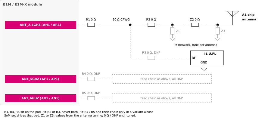
Antenna feed: link at each pad, chip antenna with π network or U.FL, 5 GHz and 6 GHz feeds not fitted
| ID | Rule | Strength | Source |
|---|---|---|---|
| CB-RF-06 | Place the 0 Ω link of each antenna pad directly on the pad landing, so a not-fitted link leaves no stub on the pad. | SHOULD | Guide (informative) |
| CB-RF-07 | Fit either the chip-antenna link or the U.FL link, never both: both together load the feed with two paths and detune the match. | SHOULD NOT | UG-E1M-001 Antenna |
| CB-RF-08 | Place a three-element π network (shunt, series, shunt) next to the antenna and tune it with a vector network analyser on the finished board in its enclosure. Until tuned, fit 0 Ω in series and leave the shunts not fitted. | SHOULD | HG-AEN-001 Wi-Fi and BLE |
| CB-RF-09 | Choose an antenna and a match that cover every band the declared SoM set uses on the feed: 2400–2483.5 MHz for all modules, plus 5150–5850 MHz and 5945–7125 MHz for E1M-X V2N and V2N-M1, which carry all bands on AR1. | SHOULD | DS-V2N-001 Wireless Module & Antenna; DS-AEN-001 RF Characteristics |
| CB-RF-10 | Before fitting a shunt inductor to GND in the π network, confirm from the SoM manifest that the feed is DC-blocked on the module. | SHOULD | Guide (informative) |
The E1M-EVK 2641-R3 shows one tuned example on E1M-AEN: a 0 Ω link to the Ignion NN02-201 chip antenna through L2 4.6 nH (shunt) and L3 2.2 nH (series), with a second shunt position (22 nH) not fitted, and a U.FL connector whose link is not fitted (UG-E1M-001 Antenna). These values are specific to that antenna, layout and enclosure.
12.3 Layout
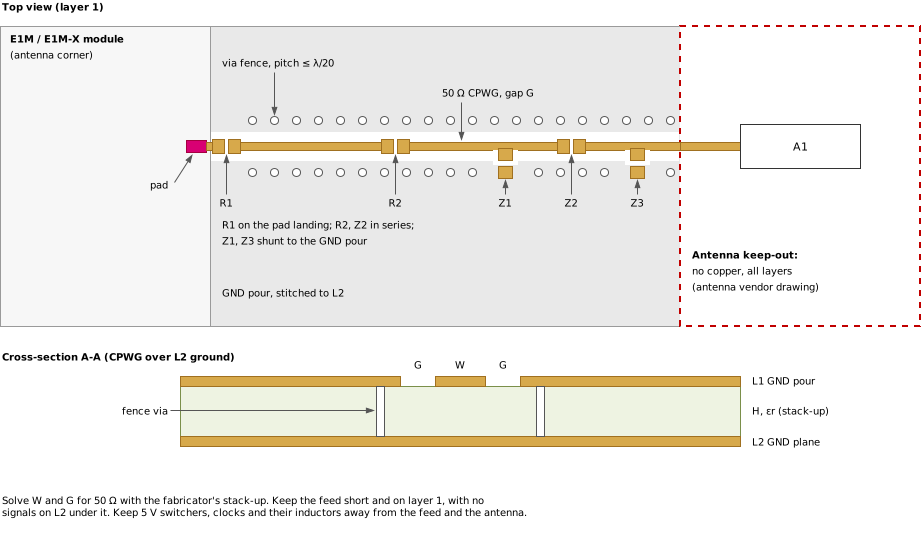
Antenna feed layout: R1 on the pad landing, R2 and Z2 in series, Z1 and Z3 shunt to the ground pour, coplanar waveguide with via fence, antenna keep-out and cross-section
| ID | Rule | Strength | Source |
|---|---|---|---|
| CB-RF-11 | Route the feed as a grounded coplanar waveguide on the top layer over a solid ground plane on layer 2. Solve trace width W and gap G for 50 Ω with the fabricator's stack-up. | SHOULD | HG-AEN-001 Wi-Fi and BLE; HG-V2N-001 Wi-Fi and BLE |
| CB-RF-12 | Surround the feed with a ground-via fence on both sides. Keep the via pitch at or below one twentieth of the wavelength at the highest frequency on the line: about 3.5 mm for 2.4 GHz only, about 1.2 mm where the line carries 6 GHz (estimated with an effective permittivity of 3). | SHOULD | Guide (informative) |
| CB-RF-13 | Keep the feed short and direct, on one layer, with no vias in it. Route no other signal on layer 2 below it. | SHOULD | HG-AEN-001 Wi-Fi and BLE |
| CB-RF-14 | Keep the antenna keep-out from the antenna vendor's drawing free of copper on all layers, and place the antenna at a board edge. | SHOULD | Guide (informative) |
| CB-RF-15 | Keep 5 V switching regulators, their inductors, clock sources and high-speed buses away from the feed and the antenna. | SHOULD | HG-AEN-001 Wi-Fi and BLE |
12.4 On-module RF connector option
Some module builds route the radio to a connector on the module instead of the antenna pad. On E1M-AEN, an I-PEX MHF 4L connector is an assembly option, not fitted in the standard build; when it is fitted, the radio output goes to it instead of AH1. On E1M-X V2N and V2N-M1, the documents list an on-module U.FL connector as an option and mark AR1 as "ANT_2.4GHz / NC". The carrier's antenna is then unused.
| ID | Rule | Strength | Source |
|---|---|---|---|
| CB-RF-16 | Check the SoM build for an on-module RF connector before relying on the carrier antenna. With such a build, keep the area above the module connector free for the cable and its mating height. | SHOULD | DS-AEN-001 Antenna Options; DS-V2N-001 Antenna Options |
12.5 Certification
The module radios carry, or are in the process of getting, modular approvals (FCC Part 15, RED / CE, ISED RSS-247, MIC). All certificate IDs and the maximum antenna gain are TBD for all three modules.
An antenna that is not listed in the module's certification report voids the modular grant, and the end product must then be certified again.
| ID | Rule | Strength | Source |
|---|---|---|---|
| CB-RF-17 | Use only an antenna type and gain listed in the certification report of every module the build variant supports, and follow the report's integration conditions (trace, gain, enclosure). | SHOULD | DS-AEN-001, DS-V2N-001, DS-V2N-M1-001 Regulatory Information |
| CB-RF-18 | Treat the E1M-EVK chip antenna (NN02-201, 4.1 dBi) as an example only. It is not shown as certified for any module. | SHOULD | HG-AEN-001 Wi-Fi and BLE |
12.6 Per-module differences
| Item | E1M-AEN | E1M-X V2N | E1M-X V2N-M1 |
|---|---|---|---|
| Radio module | BDE-BW3501N (TI CC3501E) | Murata LBEE5HY2FY (Infineon CYW55513) | as V2N |
| Wi-Fi bands | 2.4 GHz only (2412–2472 MHz) | 2400–2483.5, 5150–5850 and 5945–7125 MHz | as V2N |
| Bluetooth LE | 5.4, 2402–2480 MHz | 5.4, 2402–2480 MHz | as V2N |
| Live antenna pads | AH1 | AR1 (all bands, per the pin table) | AR1 (all bands, per the pin table) |
| Unused antenna pads | AF1, AD1: leave floating | AP1, AN1: leave floating | AP1, AN1: leave floating |
| On-module RF connector | I-PEX MHF 4L, assembly option (not fitted in the standard build) | U.FL listed as an option; build not defined | as V2N |
| Maximum antenna gain | TBD | TBD per band | TBD per band |
| Certificate IDs | TBD (FCC grant pending) | TBD (FCC grant pending) | TBD (FCC grant pending) |
| Radio ESD | ± 4 kV contact, ± 8 kV air (EN 301-489) | not stated | not stated |
| Radio power | switched, off until firmware enables Wi-Fi | not stated | not stated |
12.7 Checklist
| Check | Rule | |
|---|---|---|
| ☐ | Feed on the correct pad for the form factor (AH1 on E1M, AR1 on E1M-X). | CB-RF-01 |
| ☐ | 0 Ω link on each antenna pad; 5 GHz and 6 GHz links not fitted unless the declared SoM set drives them. | CB-RF-02, CB-RF-06 |
| ☐ | No carrier radio module; antenna pads used for RF only. | CB-RF-03, CB-RF-04 |
| ☐ | Fitted links declared per build variant. | CB-RF-05 |
| ☐ | Chip-antenna link or U.FL link fitted, not both. | CB-RF-07 |
| ☐ | π network next to the antenna, tuned on the final board; antenna covers every band in use. | CB-RF-08, CB-RF-09 |
| ☐ | 50 Ω CPWG over solid layer-2 ground, via fence, no vias in the feed, keep-out free of copper. | CB-RF-11 to CB-RF-14 |
| ☐ | Antenna listed in the certification report of every supported module. | CB-RF-17 |
13 USB
The E1M pinout has two USB groups, USB0_30 (USB 2.0 pair plus one SuperSpeed lane) and USB2 (USB 2.0 only), plus a second SuperSpeed group USB1_30 on E1M-X. The reference modules use different groups for the same job, so a carrier that hosts any module selects the group with assembly options and never connects two USB controllers to one connector.
13.1 Pad groups
| Signal | E1M pad | E1M-X pad |
|---|---|---|
USB0_30_D_P, USB0_30_D_N | B1, C1 | B1, C1 |
USB0_30_TX0_P, USB0_30_TX0_N | F1, G1 | H1, I1 |
USB0_30_RX0_P, USB0_30_RX0_N | D1, E1 | E1, F1 |
USB0_VBUS (E1M) / USB0_30_VBUS (E1M-X) | C2 | C2 |
USB0_30_ID | D2 | D2 |
USB1_30_D_P, USB1_30_D_N | (E1M-X only) | K1, L1 |
USB1_30_TX0_P, USB1_30_TX0_N | (E1M-X only) | Q1, R1 |
USB1_30_RX0_P, USB1_30_RX0_N | (E1M-X only) | N1, O1 |
USB1_30_VBUS, USB1_30_ID | (E1M-X only) | Q2, R2 |
USB2_P, USB2_N (E1M) / USB2_20_P, USB2_20_N (E1M-X) | I1, J1 | I2, J2 |
USB2_VBUS (E1M) / USB2_20_VBUS (E1M-X) | I2 | F2 |
USB2_ID (E1M) / USB2_20_ID (E1M-X) | J2 | G2 |
USB_CC1, USB_CC2 | A2, B2 | A2, B2 |
Several USB pad IDs carry different signals on the two form factors: E1M I2 is USB2_VBUS but E1M-X I2 is USB2_20_P; E1M F1 is USB0_30_TX0_P but E1M-X F1 is USB0_30_RX0_N; E1M R1 and R2 are 5 V VDD pads but E1M-X R1 and R2 are USB1_30 pads. Take every pad from the table of the form factor you are designing.
Pad domains (E1M-STD §6.7.1): the USB data pads, the VBUS pads and USB_CC1 / USB_CC2 are in the USB domain and follow the USB specifications. The ID pads are not in that list, so they are VIO_OUT-domain (1.8 V) pads and §6.2.3 applies to them.
13.2 Choosing the data group
On E1M-AEN (hw_rev R3) the only USB port is USB 2.0 on the USB0_30 pair (B1, C1), host or device. On E1M-X V2N and V2N-M1, USB0_30 is a USB 3.2 Gen 2 port and its USB 2.0 pair (B1, C1) is host-only (DS-V2N-001 USB), while USB2_20 (I2, J2) is the host-or-device USB 2.0 port. A device or OTG connector therefore sits on USB0_30 for E1M and on USB2_20 for E1M-X.
Specification conflict. E1M-STD-1.0 revision 1.4 Annex A.1 still says E1M-AEN routes "USB 2.0 only (USB2_*)", which is the hw_rev R2 state. DS-AEN-001 and HG-AEN-001 for R3 put USB 2.0 on USB0_30_D_P / USB0_30_D_N (B1 / C1), USB0_VBUS (C2) and USB0_30_ID (D2), and leave I1, J1, I2 and J2 not connected. This guide follows the module documents. A carrier designed from Annex A.1 fits the USB2 links and gets no USB on an R3 module. This guide asks for the Annex A.1 line to read: "USB 2.0 on USB0_30 D± (B1 / C1), VBUS C2, ID D2 from hw_rev R3; R2 used USB2_*" (Annex C, C-20).
Fitting the USB0_30 and the USB2 links of one connector at the same time joins two live USB controllers on one pair (both are live on E1M-X V2N), and their drivers contend.
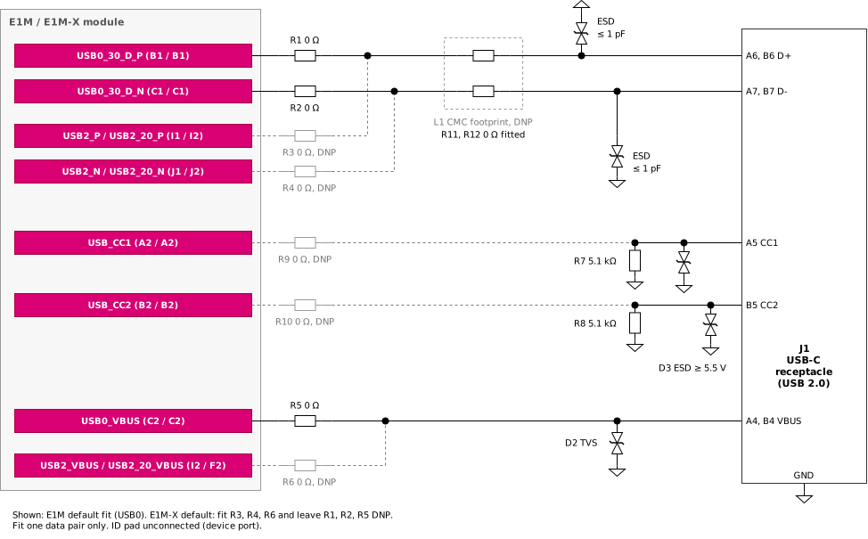
USB 2.0 device / OTG port on a USB-C receptacle: data-group links, choke footprint with 0 Ω links, ESD on D±, CC and VBUS, CC termination options and VBUS sense
| Links | E1M carrier | E1M-X carrier |
|---|---|---|
R1, R2 to USB0_30_D_P, USB0_30_D_N | fitted | not fitted |
R3, R4 to the USB2 pair | not fitted | fitted |
R5 to the USB0 VBUS pad | fitted | not fitted |
R6 to the USB2 VBUS pad | not fitted | fitted |
R7, R8 5.1 kΩ Rd on CC1, CC2 | fitted | fitted |
R9, R10 to USB_CC1, USB_CC2 | not fitted | not fitted |
| ID | Rule | Strength | Source |
|---|---|---|---|
| CB-USB-01 | Do not connect two USB controllers to one connector: fit either the USB0_30 links or the USB2 links, or use a 2:1 USB 2.0 switch (for example TMUXHS221, as on the E1M-EVK). Both links fitted make the two controllers contend on one pair, and neither port works. | SHOULD NOT | Guide (informative) |
| CB-USB-02 | Use the default fit of the table above for the form factor, and declare the fit and the supported SoMs for each build variant. | SHOULD | Guide (informative); as E1M-STD §6.7.2 (5) |
| CB-USB-03 | Do not route any other net through USB pads that one SoM leaves unconnected (for example USB_CC1, USB_CC2, the SuperSpeed lanes and the USB2 pads on E1M-AEN, or C2, D2 and all of USB1_30 on E1M-X V2N). Another SoM uses them. | MUST NOT | E1M-STD §7.3.4 |
| CB-USB-04 | For a host-only port on E1M-X, use the USB0_30 group (Figure 40); it is the only USB 3 port on V2N and V2N-M1. | SHOULD | DS-V2N-001 USB |
E1M-AEN hw_rev R2 modules used the USB2 pads (I1, J1, I2, J2) for USB 2.0. A carrier that must also take R2 modules fits the USB2 links in an R2 build variant (DS-AEN-001 Hardware Revisions).
13.3 VBUS
The VBUS pads of the reference modules are sense inputs: "connect to USB VBUS 5 V" (DS-AEN-001 USB, DS-V2N-001 USB). No module supplies VBUS. For a host port the carrier switches VBUS from its own 5 V rail.
A host cable on a device port drives 5 V into the VBUS sense pad even while the SoM is unpowered. No module document states the absolute maximum of that pad when the module is off.
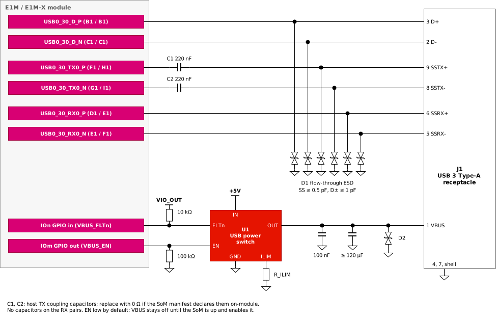
USB 3.x host port on USB0_30 with a Type-A receptacle: TX coupling capacitors, flow-through ESD and a current-limited VBUS switch
| ID | Rule | Strength | Source |
|---|---|---|---|
| CB-USB-05 | Connect a VBUS sense pad only to the VBUS of the connector of the same port. Do not connect it to any carrier supply. | MUST NOT | DS-AEN-001 USB; DS-V2N-001 USB |
| CB-USB-06 | Put a series resistor footprint between the connector VBUS and the sense pad, fitted with 0 Ω until the SoM manifest gives a limiting value. | SHOULD | Guide (informative) |
| CB-USB-07 | Supply host-port VBUS from an over-current-protected power switch fed by the carrier 5 V rail, rated at least 500 mA (USB 2.0) or 900 mA (USB 3.x) per port. Without it a shorted cable or device pulls down the carrier 5 V rail that also feeds the SoM. | MUST | USB 2.0 specification §7.2.1.2.1 and USB 3.2 specification (host over-current protection); E1M-STD §6.7.1 (USB pads per the USB specifications), §6.1.1 (1) |
| CB-USB-21 | Route the switch fault output to a SoM GPIO with a pull-up to VIO_OUT (or a rail switched by it), so firmware can report the fault. | SHOULD | Guide (informative); E1M-STD §6.2.3 (4) |
| CB-USB-08 | Hold the host VBUS switch off by default (pull-down on its enable) and let SoM firmware enable it only after VIO_OUT and PORn are high. A powered USB device on an unpowered SoM back-drives the data pads through its pull-up. | SHOULD | Guide (informative); E1M-STD §6.2.1 |
| CB-USB-09 | Fit at least 120 μF of bulk capacitance plus 100 nF on each host-port VBUS output. | SHOULD | USB 2.0 specification |
| CB-USB-10 | Size the carrier 5 V source for the host-port VBUS load in addition to the SoM peak current. | MUST | E1M-STD §6.1.1 (5) |
On the E1M-EVK 2641-R3, the USB-A host switch U8 has its enable pulled up to +5V, so its VBUS is on whenever +5V is present and the carrier I/O rail is off (UG-E1M-001 P2). CB-USB-08 avoids this.
13.4 ID and Type-C configuration channel
- ID: "Low = host, NC = device" on both module families. To force host mode, pull the
IDpad toGNDwith a 0 Ω link, a jumper or an open-drain output. For a device port leave it unconnected. - CC: E1M-AEN leaves
USB_CC1andUSB_CC2unconnected. E1M-X V2N and V2N-M1 expose them as "USB Type-C Configuration Channel", but no document says whether a CC controller is on the module or which port the pads serve. The carrier therefore terminates CC itself by default and keeps links to the CC pads as a not-fitted option.
| ID | Rule | Strength | Source |
|---|---|---|---|
| CB-USB-11 | Pull an ID pad up, if at all, only to VIO_OUT or a rail switched by it; to select host mode pull it to GND. | MUST | E1M-STD §6.2.3 (4), §6.7.1 |
| CB-USB-12 | On a USB-C device (UFP) port, fit 5.1 kΩ Rd from CC1 and from CC2 to GND and leave the links to USB_CC1 / USB_CC2 not fitted. Fit the links, and remove Rd, only for a SoM whose manifest declares CC handling, so CC is never terminated twice. | SHOULD | Guide (informative); USB Type-C specification |
| CB-USB-13 | Do not apply VBUS to a USB-C receptacle without CC attach detection. A USB-C host or dual-role port needs a CC controller (Rp, attach detection, VBUS switching); otherwise use a Type-A receptacle for host ports. | MUST NOT | USB Type-C specification |
13.5 SuperSpeed lanes
| ID | Rule | Strength | Source |
|---|---|---|---|
| CB-USB-14 | Fit AC-coupling capacitors of 75–265 nF (220 nF recommended) in the host TX pair, close to the connector side of the module, unless the SoM manifest declares them on the module; then fit 0 Ω. Fit no capacitors in the RX pair. | MUST | USB 3.2 specification (E1M-STD §6.7.1) |
| CB-USB-15 | Route the TX and RX pairs on one layer each, with no stubs, and change layers only next to ground stitching vias. | SHOULD | HG-AEN-001 Controlled-Impedance Routing |
13.6 ESD, common-mode choke and routing
| ID | Rule | Strength | Source |
|---|---|---|---|
| CB-USB-16 | Fit ESD protection on every line of every externally accessible USB connector: data, SuperSpeed, VBUS and CC. Use ≤ 0.5 pF per SuperSpeed line and ≤ 1 pF per USB 2.0 line, placed at the connector. Rate the CC protection for a working voltage of at least 5.5 V; a port that can meet sources above 5 V (USB PD, including EPR) needs CC protection rated for that VBUS level. | MUST | DS-AEN-001 ESD & Latch-up Ratings (carrier protects every external interface); Guide (capacitance and voltage values) |
| CB-USB-17 | Provide a footprint for a USB 2.0 common-mode choke (L1 in Figure 39) with 0 Ω links (R11, R12) fitted in its pads, and fit the choke instead of the links only where EMC testing needs it. | MAY | Guide (informative) |
| CB-USB-18 | Route each USB 2.0 pair as 90 Ω differential, ± 10 %. | MUST | HG-AEN-001; DS-V2N-001 USB |
| CB-USB-19 | Route each SuperSpeed pair at 85 Ω differential, ± 10 %. This value is provisional: HG-V2N-001 is the only source that gives a SuperSpeed impedance; the 90 Ω note in DS-V2N-001 applies to the USB 2.0 pair. Confirm against the SoM manifest (Annex C, C-19). | SHOULD | HG-V2N-001 USB |
| CB-USB-20 | Match the two lines of each pair to ≤ ± 2 ps (E1M-X V2N value; stricter than the ± 5 ps of E1M-AEN). | SHOULD | HG-V2N-001 USB; HG-AEN-001 |
13.7 Per-module differences
| Item | E1M-AEN (R3) | E1M-X V2N | E1M-X V2N-M1 |
|---|---|---|---|
USB0_30 USB 2.0 pair (B1, C1) | USB 2.0 FS / HS, host or device | part of the USB 3.2 Gen 2 port, host only (DS) | as V2N |
USB0_30 SuperSpeed lane | not connected | USB 3.2 Gen 2, host only (DS); HG says host or function | as V2N |
USB0 VBUS / ID (C2, D2) | VBUS sense; ID low = host, NC = device | not connected | not connected |
USB1_30 | (not on E1M) | not connected | not connected |
USB2 group | not connected (used on R2) | USB 2.0 host or device on I2, J2; VBUS F2; ID G2 | as V2N |
USB_CC1, USB_CC2 | not connected | present; owner and port not documented | as V2N |
| USB 2.0 impedance, skew | 90 Ω, ≤ ± 5 ps | 90 Ω, ≤ ± 2 ps | as V2N |
| SuperSpeed impedance | — | 85 Ω (HG-V2N-001); DS-V2N-001 silent (its 90 Ω note is for the USB 2.0 pair); open | as V2N |
| VBUS pad absolute maximum | not stated | not stated | not stated |
13.8 Checklist
| Check | Rule | |
|---|---|---|
| ☐ | Pads taken from the table of the right form factor. | — |
| ☐ | One controller per connector; default links per form factor; fit declared per variant. | CB-USB-01, CB-USB-02 |
| ☐ | No foreign net on module-unused USB pads. | CB-USB-03 |
| ☐ | VBUS sense pad only on its own connector VBUS, through a resistor footprint. | CB-USB-05, CB-USB-06 |
| ☐ | Host VBUS from an over-current-protected switch, off by default, enabled by the SoM; fault to a GPIO; 120 μF bulk. | CB-USB-07 to CB-USB-09, CB-USB-21 |
| ☐ | ID pulled only to GND or VIO_OUT. | CB-USB-11 |
| ☐ | USB-C device port: Rd fitted, CC links not fitted; no VBUS sourcing on USB-C without a CC controller. | CB-USB-12, CB-USB-13 |
| ☐ | Host TX coupling capacitors fitted (or 0 Ω if on the module); none on RX. | CB-USB-14 |
| ☐ | ESD on every connector line, CC included; choke footprint with 0 Ω links; USB 2.0 pairs 90 Ω, SuperSpeed pairs 85 Ω (provisional), ≤ ± 2 ps. | CB-USB-16 to CB-USB-20 |
14 SD Card / SDIO
The SoM supplies the SD card and protects the card bus on the module. The carrier adds the socket, a card-detect circuit and, where the card can be hot-plugged, a current limit. Everything else on the card lines is a not-fitted option.
14.1 Pads and domains
| Signal | E1M pad | E1M-X pad | Domain (E1M-STD §6.7.1) |
|---|---|---|---|
SD_CLK | AG11 | AQ31 | SD_VDD / SD_VDD_OUT |
SD_CMD | AH11 | AR31 | SD_VDD / SD_VDD_OUT |
SD_D0 | AG12 | AQ32 | SD_VDD / SD_VDD_OUT |
SD_D1 | AH13 | AR33 | SD_VDD / SD_VDD_OUT |
SD_D2 | AG13 | AQ33 | SD_VDD / SD_VDD_OUT |
SD_D3 | AH14 | AR34 | SD_VDD / SD_VDD_OUT |
SD_DET | AG14 | AQ34 | VIO_OUT (1.8 V) |
SD_RST | AH12 | AR32 | VIO_OUT (1.8 V) |
SD_VDD (E1M) / SD_VDD_OUT (E1M-X) | AH10 | AQ30 | SoM supply output |
The card lines SD_CLK, SD_CMD and SD_D0 to SD_D3 switch at the level of the SoM's card supply: 3.4 V on E1M-AEN (through its on-module NVT4858HKZ translator), 1.8 V or 3.3 V on E1M-X V2N and V2N-M1. SD_DET and SD_RST are not in that domain. E1M-STD §6.7.1 puts every signal pad that it does not list in another domain in the VIO_OUT (1.8 V) domain, with an absolute maximum of 1.98 V (§6.2.3 (5)), and DS-AEN-001 confirms 1.8 V SoC pads for E1M-AEN. The V2N and V2N-M1 documents do not state the domain of these two pads.
Three E1M-X V2N / V2N-M1 values need confirmation before a carrier relies on them. (1) DS-V2N-001 says SD_VDD_OUT switches between 1.8 V and 3.3 V; an SD card needs a VDD of 2.7–3.6 V and changes only its signalling level to 1.8 V, so the 1.8 V figure probably describes the signal level. (2) The on-module 1 MΩ pull-ups are far weaker than the 10–100 kΩ the SD specification uses; CB-SD-07 keeps carrier footprints for that case. (3) The I/O domain of SD_DET and SD_RST. If the module wires them in the RZ/V2N SD0 I/O domain (1.8 V / 3.3 V, switched), a pull-up to VIO_OUT may not reach VIH while that domain is at 3.3 V, and card detect fails. The default circuit uses the SoC internal pull-up and leaves the VIO_OUT pull-up not fitted (CB-SD-10).
A pull-up from SD_DET or SD_RST to the card supply or to 3.3 V overdrives these 1.8 V pads and can damage the SoM.
14.2 Universal circuit
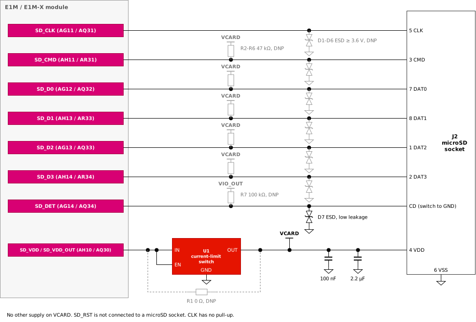
microSD reference circuit: direct card lines with not-fitted options, card detect to VIO_OUT, card supply from the SoM through a current-limit switch whose EN is tied to its input
| ID | Rule | Strength | Source |
|---|---|---|---|
| CB-SD-01 | Do not drive, back-feed or connect any carrier supply to SD_VDD (AH10) / SD_VDD_OUT (AQ30), and fit no footprint that can join a carrier rail to it in the default build. | MUST NOT | E1M-STD §6.7.1; DS-AEN-001 SD Card; DS-V2N-001 SD Card |
| CB-SD-02 | Supply the card socket VDD only from SD_VDD / SD_VDD_OUT. | MUST | E1M-STD §6.7.1; HG-AEN-001 SD Card / eMMC |
| CB-SD-03 | Where the card can be hot-plugged or its socket shorted, put a current-limited load switch (or a resettable fuse) between the pad and the socket. Choose an input range that includes 1.8 V and set the current limit at or below the SoM's rated card supply current (212 mA on E1M-AEN, 300 mA on E1M-X V2N). A card that draws more than that rating is not supported on that SoM. Tie the switch EN to its input, so that the card supply follows the SoM's card supply; do not drive EN from a carrier GPIO or rail. | SHOULD | HG-AEN-001 SD Card / eMMC; DS-AEN-001 Power Architecture |
| CB-SD-04 | Decouple the socket VDD with 100 nF and 2.2 μF (E1M-EVK values). No module states a capacitance limit for its card supply, so do not fit much more. | SHOULD | UG-E1M-001 microSD Socket; Guide (informative) |
E1M-AEN hw_rev R2 took the card supply from the carrier on AH10; from R3 AH10 is a 3.4 V output. A carrier built for R2 that supplies AH10 fights an R3 module (DS-AEN-001 Hardware Revisions). The E1M-EVK 2641-R3 keeps the R2 link R203 (0 Ω to +3V3) as not fitted; never fit it with an R3 module.
| ID | Rule | Strength | Source |
|---|---|---|---|
| CB-SD-05 | Drive or pull up SD_CLK, SD_CMD and SD_D0 to SD_D3 only to the card-supply level and only while the card supply is on. Never pull them to VIO_OUT or 3.3 V, never clamp them to VIO_OUT and never put a 1.8 V translator in the path. | MUST | E1M-STD §6.7.1 |
| CB-SD-06 | Connect the card lines straight to the socket: no series resistors and no pull-ups in the default build. Both module families have their protection and termination on the module. | SHOULD | HG-AEN-001 SD Card / eMMC; DS-V2N-001 SD Card |
| CB-SD-07 | Provide not-fitted 47 kΩ pull-up footprints from SD_CMD and SD_D0 to SD_D3 to the switched card supply (VCARD in Figure 41). Fit them only for a SoM whose manifest declares no on-module pull-ups. SD_CLK gets no pull-up. | SHOULD | Guide (informative); SD specification |
| CB-SD-08 | Give any carrier ESD diode on a card line a working voltage of at least 3.6 V. A diode rated for 1.8 V conducts at the 3.3 V or 3.4 V card level, clamps the signal and loads the card supply. | SHOULD | Guide (informative); DS-AEN-001 SD Card (3.4 V) |
| CB-SD-09 | Route the card lines short and at similar lengths over a solid ground plane. Route SD_CLK without stubs or test points. | SHOULD | Guide (informative) |
14.3 Card detect and reset
| ID | Rule | Strength | Source |
|---|---|---|---|
| CB-SD-10 | Wire the socket card-detect switch from SD_DET to GND. Use the SoC internal pull-up, or a pull-up to VIO_OUT (100 kΩ footprint, not fitted by default). Never pull SD_DET up to the card supply or to 3.3 V. | MUST | E1M-STD §6.2.3 (4), §6.7.1; HG-AEN-001 SD Card / eMMC |
| CB-SD-11 | Fit a low-capacitance, low-leakage ESD diode on SD_DET; it has no on-module protection on E1M-AEN. | SHOULD | DS-AEN-001 SD Card |
| CB-SD-12 | Leave SD_RST unconnected with a microSD socket (the card has no reset pin). It is a 1.8 V pad: an eMMC on the carrier needs its RST_n level matched to its VCCQ. | SHOULD | UG-E1M-001 microSD Socket; Guide (informative) |
Hot-plug sequence: a card inserted while the card supply is on sees VDD and the data lines at once, and its input capacitance draws an inrush through the switch. The current limit of CB-SD-03 keeps that inrush, or a shorted card, from pulling the SoM's card supply down. On E1M-AEN a short on SD_VDD resets the module repeatedly, without damage (DS-AEN-001 Power Architecture).
14.4 Per-module differences
| Item | E1M-AEN (R3) | E1M-X V2N | E1M-X V2N-M1 |
|---|---|---|---|
| Card supply pad | SD_VDD (AH10) | SD_VDD_OUT (AQ30) | SD_VDD_OUT (AQ30) |
| Card supply voltage, current | 3.4 V, 212 mA | 1.8 V / 3.3 V, switched automatically, 300 mA | as V2N |
| Card supply control | switched by firmware, off by default; no current limit on the module | not stated | not stated |
| Card-line protection on the module | NVT4858HKZ translator with EMI filter and ESD, ± 8 kV contact, ± 15 kV air | ESD, 22 Ω series resistors, 1 MΩ pull-ups | as V2N |
| Card-line level | 3.4 V (card supply), valid only while SD_VDD is on | 1.8 V or 3.3 V | as V2N |
SD_DET, SD_RST | 1.8 V SoC pads, not translated, no on-module ESD | not stated (spec default: VIO_OUT domain); to confirm | as V2N |
| On-module eMMC | none | eMMC 5.1, 4 GB (E1M-V2N101) or 16 GB | eMMC 5.1 per SKU |
| Boot from SD | no (boot ROM loads from MRAM) | Mode 0, eSD (3.3 V) | Mode 0, eSD (3.3 V) |
| hw_rev history | R2: AH10 was a carrier supply input | — | — |
14.5 Checklist
| Check | Rule | |
|---|---|---|
| ☐ | No carrier supply, link or footprint on SD_VDD / SD_VDD_OUT. | CB-SD-01 |
| ☐ | Socket VDD only from the SoM card supply, through a current limit at or below the SoM rating if hot-pluggable; switch EN tied to its input. | CB-SD-02, CB-SD-03 |
| ☐ | Card lines direct to the socket; no pull-up to VIO_OUT or 3.3 V; pull-up footprints to the card supply not fitted. | CB-SD-05 to CB-SD-07 |
| ☐ | Carrier ESD on card lines, if any, rated ≥ 3.6 V. | CB-SD-08 |
| ☐ | SD_DET to a card-detect switch to GND, pull-up only to VIO_OUT or internal; ESD fitted. | CB-SD-10, CB-SD-11 |
| ☐ | SD_RST unconnected with microSD. | CB-SD-12 |
15 Camera Interfaces (MIPI CSI-2 and Parallel)
This chapter covers the MIPI CSI-2 camera pads, the on-module camera supplies (+V_CAMx with the CAM_VFBx feedback divider), camera control (I2C, reset, master clock) and the parallel (DVP) camera pads. The rules make one carrier work with every conformant module of its form factor. Each module routes only a subset of the camera pads, so the carrier routes the full standard group and lets unused lanes float.
- On the reference modules, a loaded
+V_CAMxrail without its feedback divider regulates to its maximum and can over-volt the camera (CB-CAM-10). - A parallel camera with 2.8 V or 3.3 V I/O destroys the 1.8 V camera pads (absolute maximum 1.98 V) (CB-CAM-31).
- A camera board that pulls its reset or enable line up to 2.8 V or 3.3 V puts that voltage on a 1.8 V pad wired straight to it (CB-CAM-27).
- A camera on an always-on rail back-powers an unpowered module through its I/O (CB-CAM-18, CB-CAM-19, CB-CAM-32).
- Fitting both the carrier oscillator and the
CAM_XVCLKlink connects two clock outputs together (CB-CAM-24).
15.1 CSI pad groups
E1M defines two 4-lane CSI-2 groups (CSI0, CSI1). E1M-X defines four (CSI0 to CSI3); CSI2 and CSI3 exist only on E1M-X (E1M-STD §7.3.17). Each group has a clock pair (C) and four data pairs (0 to 3). The table lists the P / N pads of every pair.
| Pair | CSI0 E1M | CSI0 E1M-X | CSI1 E1M | CSI1 E1M-X | CSI2 E1M-X | CSI3 E1M-X |
|---|---|---|---|---|---|---|
C (clock) | P33 / P34 | R63 / R64 | V33 / V34 | X63 / X64 | AD63 / AD64 | AJ63 / AJ64 |
0 | R33 / R34 | T63 / T64 | X33 / X34 | Z63 / Z64 | AF63 / AF64 | AL63 / AL64 |
1 | Q33 / Q34 | S63 / S64 | W33 / W34 | Y63 / Y64 | AE63 / AE64 | AK63 / AK64 |
2 | O33 / O34 | Q63 / Q64 | U33 / U34 | W63 / W64 | AC63 / AC64 | AI63 / AI64 |
3 | N33 / N34 | P63 / P64 | T33 / T34 | V63 / V64 | AB63 / AB64 | AH63 / AH64 |
The camera supplies belong to the power and control pads (E1M-STD §7.3.1):
| Pad name | E1M | E1M-X | Function |
|---|---|---|---|
+V_CAM0 | Z34 | H64 | Camera LDO output 0 |
CAM_VFB0 | Z33 | H63 | Feedback node of +V_CAM0 (reference modules; function not defined in E1M-STD-1.0 revision 1.4) |
+V_CAM1 | AB34 | J64 | Camera LDO output 1 |
CAM_VFB1 | AB33 | J63 | Feedback node of +V_CAM1 |
+V_CAM2 | — | L64 | Camera LDO output 2 (E1M-X only) |
CAM_VFB2 | — | L63 | Feedback node of +V_CAM2 (E1M-X only) |
+V_CAM3 | — | N64 | Camera LDO output 3 (E1M-X only) |
CAM_VFB3 | — | N63 | Feedback node of +V_CAM3 (E1M-X only) |
15.2 Universal connector wiring and routing
Route the clock and all four data pairs of every CSI group the carrier uses to the camera connector. A module that implements fewer lanes leaves the remaining pads unconnected; the carrier traces to them then float, which is harmless. A pad that one module does not route is still a standard CSI pad on another module, so it never carries another net.
| ID | Strength | Rule | Source |
|---|---|---|---|
| CB-CAM-01 | MUST NOT | Route an unrelated net through a CSI pad that a module does not route (for example E1M-AEN CSI0 lanes 2 / 3 and all of CSI1, or E1M-X V2N CSI2 / CSI3). These pads keep their CSI function on other modules. | E1M-STD §7.3.4, §9.2 (9) |
| CB-CAM-02 | SHOULD | Route the clock pair and all four data pairs of each CSI group the carrier uses to the connector, with no termination, pull or bias on the lanes. Lanes the module does not drive float. | Guide (informative) |
| CB-CAM-03 | SHOULD | Choose sensors that can run in the lane count of every module the carrier targets. A sensor that works only in 4-lane mode does not work on E1M-AEN (2 lanes). Declare a narrower SoM set if the sensor needs 4 lanes. | DS-AEN-001; E1M-STD §9.2 (2) |
| CB-CAM-04 | MUST | Treat the CSI pads as high-speed differential pads: do not clamp them to VIO_OUT, pull them up or level-translate them. Route them as the MIPI D-PHY specification requires. | E1M-STD §6.7.1 |
| CB-CAM-05 | SHOULD | Route each pair as 100 Ω differential, ± 10 %. Match length within each pair first, then match every data pair to the clock pair of its group. Keep the pairs on one layer over a continuous ground plane, minimise vias and avoid stubs. | HG-AEN-001 MIPI CSI-2; HG-V2N-001 MIPI CSI-2 |
| CB-CAM-06 | SHOULD NOT | Swap the P and N of a pair or reorder lanes to ease routing. The specification defines no lane or polarity swap, so a swap works only on a module that declares support for it. | E1M-STD §7.3.17; Guide (informative) |
| CB-CAM-07 | SHOULD | Fit a low-capacitance TVS array on every pair at the camera connector. No module has CSI ESD protection on the module. | HG-AEN-001 MIPI CSI-2; HG-V2N-001 rev 0.2 |
| CB-CAM-08 | SHOULD NOT | Split a CSI pair passively to two connectors. To share one CSI group between connectors, use a MIPI switch (the E1M EVK uses PI3WVR626XEBEX). | HG-AEN-001 MIPI CSI-2 |
On E1M-AEN hardware revision R2, the P and N pads of each CSI-2 lane are swapped on the module. The pad polarity in this guide and in E1M-STD §7.3.17 matches R3 and later (DS-AEN-001). A carrier built to this guide receives inverted lanes from an R2 module.
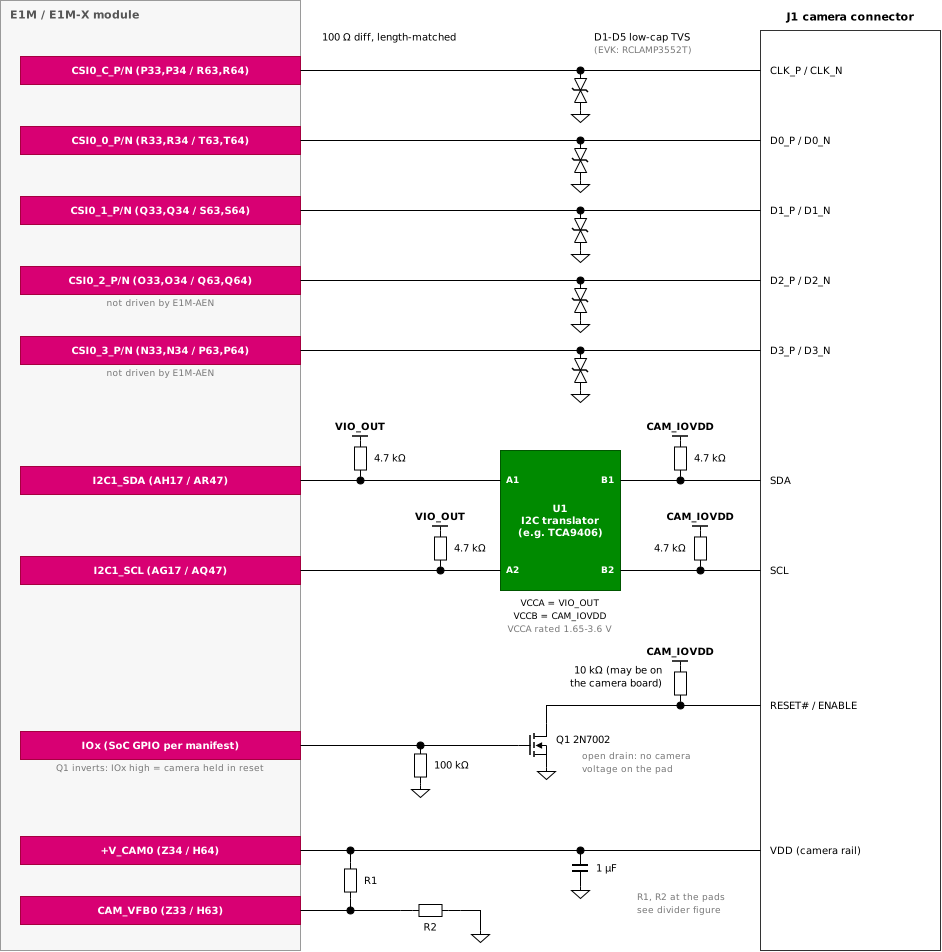
CSI-2 camera reference: all four lanes and the clock of CSI0 with low-capacitance TVS at the connector, camera I2C through a translator referenced to VIO_OUT, camera reset / enable through the open-drain N-MOSFET Q1 (gate held low by default), and +V_CAM0 with its feedback divider at the pads (E1M pad / E1M-X pad)
15.3 Camera supplies (+V_CAMx and CAM_VFBx)
On the reference modules (E1M-AEN, E1M-X V2N and V2N-M1), each +V_CAMx pad is the output of an adjustable LDO with a 0.6 V reference, and the carrier sets the output voltage with a resistor divider from +V_CAMx to CAM_VFBx (R1) and from CAM_VFBx to GND (R2). E1M-STD-1.0 revision 1.4 lists +V_CAM0–+V_CAM3 as SoM supply outputs (§6.7.1) but defines neither the function of CAM_VFBx, the reference voltage nor the output range; the rules below apply to a SoM that declares an external-divider LDO, as every reference module does.
VCAM = 0.6 V × (1 + R1 / R2)
Size the divider so that its current is at least 100 times the maximum feedback-pin current:
R1 + R2 ≤ VCAM / (IFB,max × 100)
E1M-AEN gives IFB,max = 100 nA (10 nA nominal). The E1M-X V2N and V2N-M1 documents do not give IFB; until they do, use 100 nA for every module.
| VCAM | R1 | R2 | R1 + R2 (limit at 100 nA) |
|---|---|---|---|
| 2.8 V | 110 kΩ | 30 kΩ | 140 kΩ (≤ 280 kΩ) |
| 1.8 V | 20 kΩ | 10 kΩ | 30 kΩ (≤ 180 kΩ) |
| 1.2 V | 10 kΩ | 10 kΩ | 20 kΩ (≤ 120 kΩ) |
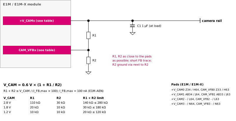
Camera LDO feedback divider: R1 from +V_CAMx to CAM_VFBx, R2 from CAM_VFBx to GND, both next to the pads, with the formula, the divider-current limit and worked values
| ID | Strength | Rule | Source |
|---|---|---|---|
| CB-CAM-10 | MUST | For a SoM that declares an external-divider LDO on +V_CAMx (every reference module), fit the R1 / R2 divider on every +V_CAMx pad that is connected to a load. Without it, a firmware-enabled LDO has a floating feedback node, regulates to its maximum and can over-volt the camera. Make the divider fitted in the default assembly; leave it unfitted only in a build variant whose SoMs declare a fixed or internally set output. | HG-AEN-001 MIPI CSI-2; DS-V2N-001; Guide (damage) |
| CB-CAM-11 | SHOULD | Place R1 and R2 as close to the +V_CAMx and CAM_VFBx pads as possible, keep the feedback trace short and away from switching nodes, and give R2 its own ground via. A long feedback trace can make the LDO oscillate. | HG-AEN-001; DS-V2N-001; AN-003 |
| CB-CAM-12 | SHOULD | Set VCAM to 0.6–3.1 V, the narrowest range of the reference modules (E1M-AEN), on every carrier. An E1M-X carrier MAY use settings up to 3.3 V only in a build variant that declares a SoM set of E1M-X V2N / V2N-M1. | DS-AEN-001; DS-V2N-001; E1M-STD §9.2 (2) |
| CB-CAM-13 | MUST | Keep the camera load within the current the SoM declares for +V_CAMx: on E1M-AEN, ≤ 170 mA for +V_CAM0 and +V_CAM1 combined and ≤ 100 mA per rail at a 3.1 V setting (about 96 mA per rail at a 1.2 V setting at TA = 75 °C); on E1M-X V2N / V2N-M1, ≤ 300 mA per rail. Use a carrier regulator for larger loads. | DS-AEN-001; HG-AEN-001 Camera Rails; DS-V2N-001; Guide (module stress) |
| CB-CAM-14 | MUST NOT | Connect another supply to +V_CAMx, drive CAM_VFBx from a carrier circuit, or back-feed either pad. | +V_CAMx: E1M-STD §6.7.1; CAM_VFBx: DS-AEN-001, DS-V2N-001 (not covered by E1M-STD-1.0 revision 1.4) |
| CB-CAM-15 | SHOULD | Size the divider with R1 + R2 ≤ VCAM / (IFB,max × 100), using 100 nA where the module gives no value. | HG-AEN-001; HG-V2N-001 |
| CB-CAM-16 | MAY | Add decoupling at the camera connector. The module documents give no capacitance limit for +V_CAMx; the E1M EVK fits 10 μF + 2.2 μF per rail. | EVK user guide (informative) |
| CB-CAM-17 | SHOULD | Expect the +V_CAMx rails to be off until firmware enables them, and plan any sensor supply order in firmware. Where a sensor needs a supply order the firmware cannot give, supply it from carrier load switches instead. | DS-AEN-001; Guide (informative) |
| CB-CAM-18 | MUST | Keep every camera supply that powers circuits driving VIO_OUT-domain pads (parallel camera data and sync, I2C, control) off while VIO_OUT is low: use +V_CAMx, or a carrier rail switched by VIO_OUT. | E1M-STD §6.2.3 (1), §6.1.2 (3) |
| CB-CAM-19 | SHOULD | Power CSI-2 sensors from +V_CAMx or from a carrier rail switched by VIO_OUT, not from an always-on rail, so that a powered sensor does not drive D-PHY levels into an unpowered module. | Guide (informative) |
On E1M-X V2N and V2N-M1 there are four camera LDOs but only two CSI groups (CSI0, CSI1). The documents do not say which LDO is meant for which camera. Any +V_CAMx can supply any camera; this guide uses +V_CAM0 for CSI0 and +V_CAM1 for CSI1 and leaves +V_CAM2 / +V_CAM3 for additional camera rails.
15.4 Camera control: I2C, reset and master clock
The specification assigns no camera I2C bus, reset or power-down pad and no master clock to the CSI groups. The carrier picks them from the standard pads and records the choice in its build files (device tree, board description).
| ID | Strength | Rule | Source |
|---|---|---|---|
| CB-CAM-20 | MUST | Pull the module side of the camera I2C bus up only to VIO_OUT. Where the camera I/O is not 1.8 V, use a translator with VCCA = VIO_OUT whose ports stay high-impedance while VCCA is off. Choose a translator whose VCCA is rated 1.65–3.6 V (CB-IO-22, informative); VIO_OUT stays 1.8 V in this revision. | E1M-STD §6.2.3 (4), §6.1.2 (5) |
| CB-CAM-21 | SHOULD | Use a standard I2C instance for the camera (the E1M EVK uses I2C1: E1M AG17 / AH17, E1M-X AQ47 / AR47) and check the module's on-module I2C addresses before adding devices to that bus (see the I2C rules in the serial-interfaces chapter). | E1M-STD §7.3.8; EVK user guide |
| CB-CAM-22 | MUST | Drive camera reset, power-down and oscillator enable from SoC-owned GPIOs. Where the chosen pad needs a function beyond its default and GPIO secondary, declare it as a per-SoM dependency. On E1M-AEN, IO13 and IO15–IO24 are not SoC GPIOs (Wi-Fi module GPIOs or not bonded); on E1M-X V2N-M1, IO0–IO6, IO17–IO22 and IO24 are routed to the on-module DX-M1. | E1M-STD §8.4, §9.2 (2); DS-AEN-001; DS-V2N-M1-001 |
| CB-CAM-27 | MUST | Where the camera I/O is not 1.8 V, or the camera board may carry its own pull-up, drive camera reset, power-down and enable through an open-drain N-MOSFET (gate from the GPIO, gate pull-down to GND) or a fixed-direction translator with VCCA = VIO_OUT and Ioff. Never wire such a line straight to a pad: a 2.8 V or 3.3 V camera-side pull-up exceeds the 1.98 V pad maximum and back-powers an unpowered module. The E1M EVK drives CAM_EN_# this way through Q1. | E1M-STD §6.2.3 (1), (5); E1M EVK user guide |
| CB-CAM-23 | SHOULD | Where a 1.8 V reset line is driven directly, hold camera reset asserted by default with a 100 kΩ pull-down on the camera side. Where an inverting N-MOSFET drives it (CB-CAM-27), keep the camera unpowered until firmware has set the reset GPIO. Pull-downs are permitted at any time. | E1M-STD §6.2.3 (1), (3); Guide (informative) |
| CB-CAM-24 | MUST | Fit exactly one master-clock source per camera: the carrier oscillator (RA) or the CAM_XVCLK link (RB), never both. Two clock outputs on one net contend. | Guide (damage) |
| CB-CAM-25 | SHOULD | Make the carrier oscillator the default fit. Fit the CAM_XVCLK link only in a build variant whose SoMs declare a CAM_XVCLK output; on E1M-X V2N and V2N-M1 the pad is not connected. | DS-V2N-001; E1M-STD §6.7.2 (1) (by analogy) |
| CB-CAM-26 | SHOULD | Power the oscillator from a rail switched by VIO_OUT and gate its output enable from a GPIO with a pull-down, so that no clock reaches the camera or the module while VIO_OUT is low, and firmware starts the clock only after PORn is high. | E1M-STD §6.2.3 (1), (3); Guide (informative) |
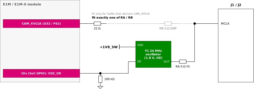
Camera master-clock option: a 1.8 V oscillator with GPIO output enable through RA (default fit), or CAM_XVCLK through RB (not fitted unless the SoM declares the output); fit exactly one
15.5 ESD and connector sharing
- Put the TVS array at the connector, with the shortest possible path to ground. The pairs see the TVS capacitance, so choose a part specified for MIPI D-PHY data rates (CB-CAM-07).
- Protect the low-speed camera lines (I2C, reset, master clock) at the connector with low-capacitance ESD diodes rated for the camera I/O level.
- Do not hot-plug camera flat cables; the E1M EVK user guide gives the same instruction for its camera connectors.
15.6 Parallel camera (DVP)
E1M exposes an 8-bit parallel camera (CAM_D1–CAM_D8); E1M-X exposes 16 bits (CAM_D1–CAM_D16). Both add CAM_HSYNC, CAM_VSYNC, CAM_PCLK and CAM_XVCLK (E1M-STD §7.3.18). The data pads are numbered from CAM_D1; there is no CAM_D0 pad.
| Pad name | E1M | E1M-X | Direction (module) |
|---|---|---|---|
CAM_D1–CAM_D8 | W32, X32, Y32, Z32, AA32, AB32, AC32, AD32 | G62, H62, I62, J62, K62, L62, M62, N62 | input |
CAM_D9–CAM_D16 | — | O62, P62, Q62, R62, S62, T62, U62, V62 | input (E1M-X only) |
CAM_HSYNC | T32 | C62 | input |
CAM_VSYNC | S32 | D62 | input |
CAM_PCLK | V32 | E62 | input (pixel clock from the sensor) |
CAM_XVCLK | U32 | F62 | output (sensor master clock) |
| ID | Strength | Rule | Source |
|---|---|---|---|
| CB-CAM-30 | MUST NOT | Route an unrelated net through a parallel-camera pad that a module does not route. On E1M-X V2N and V2N-M1, every parallel-camera pad is not connected but keeps its function on other modules. | E1M-STD §7.3.4 |
| CB-CAM-31 | MUST | Use a sensor whose I/O supply (DOVDD) is 1.8 V, or translate its outputs to 1.8 V. The parallel-camera pads are VIO_OUT-domain pads with an absolute maximum of −0.3 V to 1.98 V; 2.8 V or 3.3 V sensor I/O destroys them. | E1M-STD §6.2.3 (5), §6.7.1 |
| CB-CAM-32 | MUST | Supply the sensor DOVDD from a VIO_OUT-switched carrier 1.8 V rail (a load switch with its enable on VIO_OUT) or from +V_CAMx, never from an always-on rail. | E1M-STD §6.2.3 (1), §6.1.2 (3) |
| CB-CAM-33 | SHOULD | Fit a series resistor (22–33 Ω) at the source of each clock: at the connector for CAM_PCLK (driven by the sensor), at the pad for CAM_XVCLK (driven by the module). | Guide (informative) |
| CB-CAM-34 | SHOULD | Length-match CAM_Dx, CAM_HSYNC and CAM_VSYNC to CAM_PCLK, and keep the bus away from the MIPI pairs and switching nodes. | Guide (informative) |
| CB-CAM-35 | SHOULD | Confirm the bit order against the SoM manifest before layout. The specification does not say which CAM_Dx pad is the least significant bit. The E1M EVK connects its connector CAM_D0 to pad AD32 (CAM_D8) and CAM_D7 to W32 (CAM_D1). | E1M-STD §7.3.18; EVK user guide |
| CB-CAM-36 | SHOULD | On E1M-X, check in the SoM manifest which 8 of the 16 data pads an 8-bit sensor uses before routing an 8-bit sensor. | Guide (informative) |
| CB-CAM-37 | MUST | Keep the sensor outputs (CAM_Dx, CAM_HSYNC, CAM_VSYNC, CAM_PCLK) high-impedance until the module may receive them: hold the sensor in reset or power-down (CB-CAM-23) and its master clock gated off (CB-CAM-26) until firmware releases them after PORn is high. A sensor on a VIO_OUT-switched rail is powered as soon as VIO_OUT rises, before PORn is high. | E1M-STD §6.2.3 (3) |
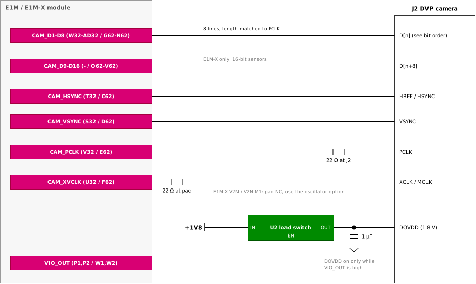
Parallel (DVP) camera reference: data bus, sync, CAM_PCLK with series resistor at the connector, CAM_XVCLK with series resistor at the pad, and 1.8 V sensor I/O from a load switch enabled by VIO_OUT (E1M pad / E1M-X pad)
15.7 Per-module differences
| Item | E1M-AEN | E1M-X V2N | E1M-X V2N-M1 |
|---|---|---|---|
| CSI groups routed | CSI0, 2 lanes (lanes 2 / 3 and all of CSI1 not routed) | CSI0 and CSI1, 4 lanes each (CSI2 / CSI3 not connected) | As V2N |
| CSI-2 performance | Up to 2.5 Gbps per lane; up to 2 MP input; 16 virtual channels | Up to 4K @ 30 fps; 4 virtual channels | As V2N |
| Camera LDOs | 2 (+V_CAM0, +V_CAM1, TLV77201) | 4 (+V_CAM0–+V_CAM3) | As V2N |
| LDO type | Adjustable, external divider on CAM_VFBx | Adjustable, external divider on CAM_VFBx | As V2N |
| LDO range | 0.6–3.1 V | 0.6–3.3 V | 0.6–3.3 V |
| LDO current | 170 mA combined; 100 mA per rail at 3.1 V | 300 mA per rail | 300 mA per rail |
IFB,max of CAM_VFBx | 100 nA (10 nA nominal) | Not stated | Not stated |
| LDO default state | Off until firmware enables it | Not stated | Not stated |
| LDO-to-camera mapping | Either rail, any camera | Not stated | Not stated |
CAM_XVCLK | U32, sensor master clock output | F62 not connected | F62 not connected |
| Parallel camera | 8-bit, live (CAM_D1–CAM_D8, sync, CAM_PCLK, CAM_XVCLK) | Not connected | Not connected |
| CSI ESD on module | None | None (moved to the carrier, HG rev 0.2) | None |
| hw_rev note | R2: P / N of each CSI lane swapped on the module | — | — |
15.8 Chapter checklist
| Done | Check | Rule |
|---|---|---|
| ☐ | Clock and all four data pairs of each used CSI group reach the connector; no termination or bias on the lanes. | CB-CAM-02 |
| ☐ | No unrelated net on a CSI or parallel-camera pad that a module does not route. | CB-CAM-01, CB-CAM-30 |
| ☐ | Sensor lane count works on every targeted module, or the SoM set is declared. | CB-CAM-03 |
| ☐ | Pairs 100 Ω ± 10 %, intra-pair matched, data matched to clock; no P / N swaps. | CB-CAM-05, CB-CAM-06 |
| ☐ | Low-capacitance TVS on every pair at the connector; MIPI switch, not a passive split, for shared ports. | CB-CAM-07, CB-CAM-08 |
| ☐ | R1 / R2 divider fitted on every loaded +V_CAMx, next to the pads; VCAM 0.6–3.1 V (up to 3.3 V only in a declared V2N / V2N-M1 variant). | CB-CAM-10 to CB-CAM-12 |
| ☐ | Camera load within the declared limit: E1M-AEN ≤ 170 mA combined, ≤ 100 mA per rail at 3.1 V, about 96 mA per rail at 1.2 V (TA = 75 °C); E1M-X ≤ 300 mA per rail. | CB-CAM-13 |
| ☐ | No supply or driver on +V_CAMx or CAM_VFBx. | CB-CAM-14 |
| ☐ | Camera supplies follow the module (+V_CAMx or VIO_OUT-switched rails). | CB-CAM-18, CB-CAM-19, CB-CAM-32 |
| ☐ | Camera I2C pulled up to VIO_OUT on the module side; translator high-impedance when unpowered, VCCA rated 1.65–3.6 V. | CB-CAM-20 |
| ☐ | Reset and enable on SoC-owned GPIOs, through an open-drain N-MOSFET or translator where the camera I/O is not 1.8 V; reset held by default. | CB-CAM-22, CB-CAM-23, CB-CAM-27 |
| ☐ | Exactly one master-clock source fitted; oscillator is the default. | CB-CAM-24, CB-CAM-25 |
| ☐ | Parallel camera I/O at 1.8 V; series resistors on CAM_PCLK and CAM_XVCLK; bit order confirmed. | CB-CAM-31, CB-CAM-33, CB-CAM-35 |
| ☐ | Sensor held in reset with its clock gated until after PORn is high. | CB-CAM-37 |
16 Display Interfaces and Backlight
This chapter covers the MIPI DSI display pads, the panel supplies and control lines that the carrier provides, the backlight pads (BL_LED_A, BL_LED_K) and the E1M-X parallel LCD pads. The module drives the DSI lanes and, on the reference modules, an on-module backlight boost converter. Every other panel supply comes from the carrier.
BL_LED_Acarries the backlight boost output, up to 36 V on E1M-AEN; a logic input, a supply or a low-voltage part on it is destroyed (CB-DSP-12, CB-DSP-13).- Two feedback resistors in the LED return (one on the module, one on the carrier) over-drive the LED string (CB-DSP-14).
- Sizing RFB for E1M-AEN with the 95 mV formula of DS-AEN-001 sets about 2.1 times the intended LED current; the KTD2801 regulates its feedback to 200 mV. The E1M-X 95 mV value is unverified and may carry the same error (CB-DSP-15).
- Fitting the on-module boost path and the carrier backlight-driver path together connects two drivers to one LED string (CB-DSP-18).
16.1 DSI pad groups
Both form factors define two 4-lane DSI groups, DSI0 and DSI1 (E1M-STD §7.3.16). The backlight pads are power and control pads (E1M-STD §7.3.1).
| Pair | DSI0 E1M | DSI0 E1M-X | DSI1 E1M | DSI1 E1M-X |
|---|---|---|---|---|
C (clock) | D33 / D34 | A57 / B57 | J33 / J34 | A49 / B49 |
0 | F33 / F34 | A61 / B61 | L33 / L34 | A53 / B53 |
1 | E33 / E34 | A60 / B60 | K33 / K34 | A52 / B52 |
2 | C33 / C34 | A59 / B59 | I33 / I34 | A51 / B51 |
3 | B33 / B34 | A58 / B58 | H33 / H34 | A50 / B50 |
| Pad name | E1M | E1M-X | Function |
|---|---|---|---|
BL_LED_A | A31 | B55 | Backlight boost output, LED string anode. |
BL_LED_K | B31 | A55 | LED string cathode and feedback node. |
16.2 Universal panel connector wiring
Route the clock and all four data pairs of DSI0 to the panel connector. Route DSI1 only if the carrier has a second panel connector; no current module drives DSI1.
| ID | Strength | Rule | Source |
|---|---|---|---|
| CB-DSP-01 | MUST NOT | Route an unrelated net through a DSI pad that a module does not route (E1M-AEN DSI0 lanes 2 / 3 and all of DSI1; E1M-X V2N / V2N-M1 all of DSI1). | E1M-STD §7.3.4, §9.2 (9) |
| CB-DSP-02 | SHOULD | Route the clock pair and all four data pairs of DSI0 to the panel connector, with no termination, pull or bias. Lanes the module does not drive float. | Guide (informative) |
| CB-DSP-03 | SHOULD | Choose panels that run in the lane count and lane rate of every module the carrier targets. A panel that needs 4 lanes does not work on E1M-AEN (2 lanes, 1.25 Gbps per lane, video mode only). Declare a narrower SoM set if the panel needs 4 lanes. | DS-AEN-001; E1M-STD §9.2 (2) |
| CB-DSP-04 | MUST | Treat the DSI pads as high-speed differential pads: do not clamp them to VIO_OUT, pull them up or level-translate them. Route them as the MIPI D-PHY specification requires. | E1M-STD §6.7.1 |
| CB-DSP-05 | SHOULD | Route each pair as 100 Ω differential, ± 10 %. Match length within each pair, then match every data pair to the clock pair. Minimise vias and stubs over a continuous ground plane. | HG-AEN-001 MIPI DSI; HG-V2N-001 MIPI DSI |
| CB-DSP-06 | SHOULD | Fit a low-capacitance TVS array on every pair at the panel connector. No module has DSI ESD protection on the module. | HG-AEN-001 MIPI DSI; HG-V2N-001 rev 0.2 |
| CB-DSP-07 | SHOULD NOT | Split a DSI pair passively to two connectors; use a differential switch (the E1M EVK uses PI3DBS12212AXUAEX). | HG-AEN-001 MIPI DSI |
| CB-DSP-08 | SHOULD NOT | Swap the P and N of a pair or reorder lanes; the specification defines no lane or polarity swap. | E1M-STD §7.3.16; Guide (informative) |
16.3 Panel power, reset and tearing effect
The module supplies no panel logic or analogue rail. The carrier generates the panel I/O rail (VDDI, typically 1.8 V) and the panel analogue rail (VCI / AVDD, typically 2.8–3.3 V) and switches them so that they follow the module.
| ID | Strength | Rule | Source |
|---|---|---|---|
| CB-DSP-09 | MUST NOT | Supply the panel from VIO_OUT directly. A panel rail that must follow the module comes from a carrier load switch whose enable is VIO_OUT (or is gated by it). | E1M-STD §6.1.2 (3), (4) |
| CB-DSP-10 | MUST | Pull the module side of panel reset, tearing effect (TE), touch interrupt and touch I2C up only to VIO_OUT. Where the panel I/O is not 1.8 V, use a translator with VCCA = VIO_OUT that is high-impedance while VCCA is off. Choose a translator whose VCCA is rated 1.65–3.6 V (CB-IO-22, informative); VIO_OUT stays 1.8 V in this revision. | E1M-STD §6.2.3 (4), §6.1.2 (5) |
| CB-DSP-11 | SHOULD | Hold panel power off by default with a pull-down on each load-switch enable (the E1M EVK fits R65 10 kΩ on LCD_PWR_EN). Hold panel reset asserted by default with a 100 kΩ pull-down. Drive reset and the power enables from SoC-owned GPIOs, and wire TE to a GPIO input. | Power enable: E1M EVK user guide; reset: Guide (informative); E1M-STD §6.2.3 (1) |
| CB-DSP-21 | MUST | Keep the panel from driving VIO_OUT-domain pads (TE, touch interrupt) before the module may receive them: keep the panel unpowered or in reset until firmware releases it after PORn is high, so that its outputs stay high-impedance. | E1M-STD §6.2.3 (1), (3) |
The E1M EVK (2641-R3) differs on panel reset: it pulls LCD_RST up with R83 (100 kΩ to +VIO_SW), so the panel leaves reset as soon as +VIO_SW is on. Its panel power stays off by default through R65, which keeps the panel outputs inactive. CB-DSP-11 recommends a reset pull-down as well.
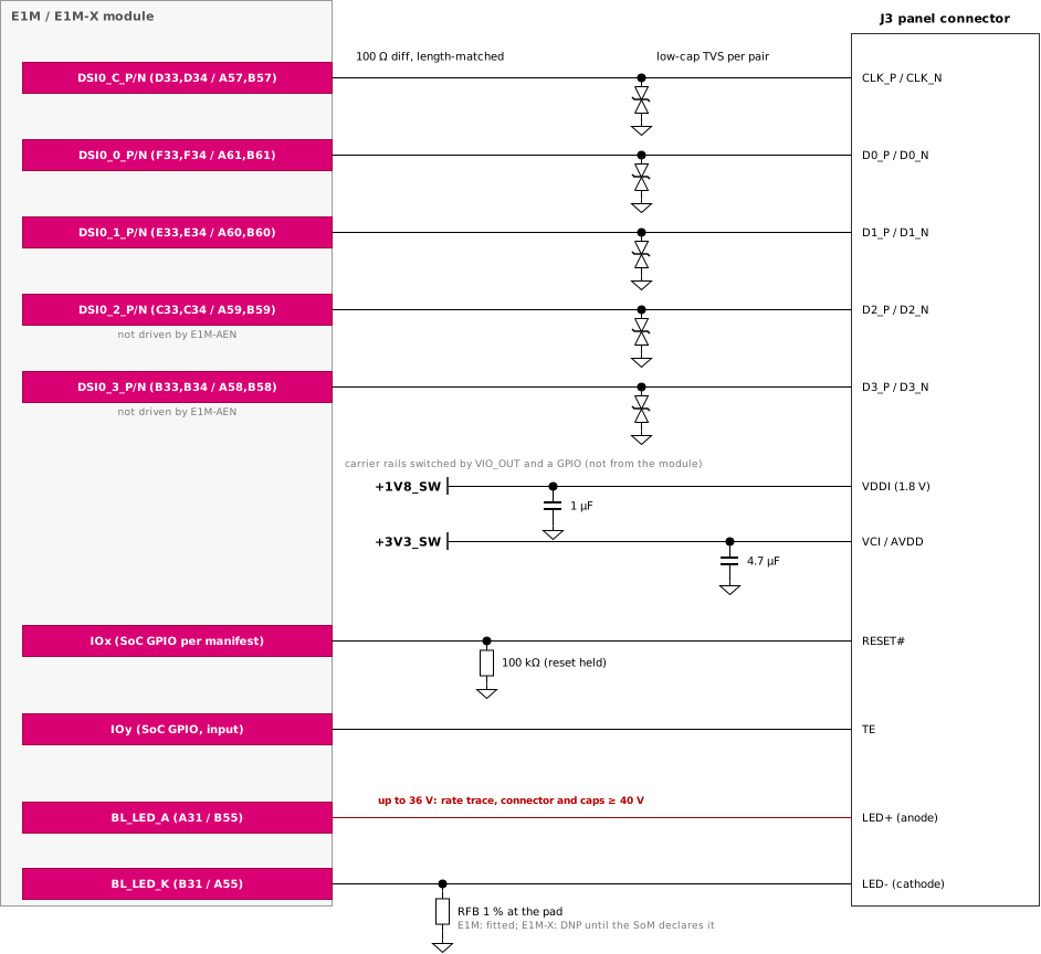
DSI panel reference: clock and four data pairs with TVS at the connector, carrier panel rails switched to follow the module, reset held by a pull-down, TE to a GPIO, and the backlight anode and cathode with RFB at the pad (fitted on E1M; not fitted on E1M-X until the SoM declares it) (E1M pad / E1M-X pad)
16.4 Backlight
The reference modules fit an optional backlight boost converter on the module. Its output drives the LED string anode on BL_LED_A; the string cathode returns on BL_LED_K through one feedback resistor RFB to GND, which sets the LED current. E1M-STD §6.7.1 allows only an LED string and its feedback network on these two pads. A carrier that needs its own backlight driver takes the PWM from a standard PWM pad (E1M-STD §7.3.24) and keeps the driver off BL_LED_A. The carrier supports both paths with assembly options; the default fit is the one that cannot damage anything when an unknown module is fitted.
For E1M-AEN, the converter is a Kinetic KTD2801ECD-TR: its feedback regulates to 200 mV (184 mV minimum, 216 mV maximum), its over-voltage threshold is 36 V and its VOUT absolute maximum is 40 V (KTD2801 datasheet rev 04c). The LED current is:
ILED = VFB / RFB = 200 mV / RFB
For example, a 20 mA string needs RFB = 10 Ω; the worst-case current is then 216 mV / 10 Ω = 21.6 mA.
The E1M-X V2N and V2N-M1 documents give ILED = 95 mV / RFB for their driver, but name neither the part, its over-voltage threshold nor the location of RFB. DS-AEN-001 gives the same 95 mV for the KTD2801, which is wrong. This guide therefore treats the E1M-X 95 mV as unverified: if the E1M-X driver is also a KTD2801, an RFB sized from 95 mV sets about 2.1 times the intended LED current.
| ID | Strength | Rule | Source |
|---|---|---|---|
| CB-DSP-12 | MUST | Connect only the LED string anode to BL_LED_A and only the string cathode and its feedback network to BL_LED_K. Never connect a logic input (including a backlight-driver PWM input), another supply or a GPIO function to either pad. This also applies to the BL_PWM output that DS-AEN-001 and DS-V2N-001 describe for module builds without the on-module driver; E1M-STD-1.0 revision 1.4 defines no such option. | E1M-STD §6.7.1, §9.2 (8) |
| CB-DSP-13 | MUST | Rate every part on BL_LED_A (trace spacing, connector pins, any capacitor) for at least the greater of 40 V and the BL_LED_A maximum the SoM declares. On E1M-AEN the boost output reaches the 36 V over-voltage threshold when the string is open (VOUT absolute maximum 40 V). The E1M-X V2N / V2N-M1 value is not stated and is unconfirmed. | E1M-STD §6.7.1 (informative note); DS-AEN-001; KTD2801 datasheet |
| CB-DSP-22 | SHOULD NOT | Fit a TVS or ESD diode on BL_LED_A. If one is fitted, its reverse stand-off voltage must be at least the over-voltage maximum the SoM declares (36 V on E1M-AEN), so that it never conducts in normal operation. Such a part clamps above the 40 V VOUT absolute maximum, so it does not protect the module. | Guide (informative); KTD2801 datasheet |
| CB-DSP-14 | MUST | Fit exactly one feedback resistor in the LED return. On E1M-AEN, RFB is on the carrier between BL_LED_K (B31) and GND. On E1M-X, fit the carrier RFB only for SoMs that declare the feedback resistor off-module; the V2N / V2N-M1 location is not documented, so keep it a not-fitted option until confirmed. | HG-AEN-001 MIPI DSI; Guide (damage) |
| CB-DSP-15 | MUST | Size RFB from the feedback voltage the SoM declares. For E1M-AEN use 200 mV (KTD2801), not the 95 mV of DS-AEN-001; check the string rating at VFB,max = 216 mV. For E1M-X, do not rely on the 95 mV of DS-V2N-001 / HG-V2N-001 until Alp Lab confirms the driver part; check the string rating at up to 216 mV. | HG-AEN-001; KTD2801 datasheet; DS-V2N-001 (unverified) |
| CB-DSP-16 | SHOULD | Place RFB next to the BL_LED_K pad with its own ground via, use a 1 % part, and keep the LED anode and cathode traces together to keep the boost current loop small. | Guide (informative); E1M-AEN EMC pre-compliance |
| CB-DSP-17 | SHOULD | Keep the LED string within the driver limits: up to 10 LEDs in series or 2P6S, with the string forward voltage at maximum current clearly below the over-voltage threshold (36 V on E1M-AEN; not stated for E1M-X). Limit the backlight LED power to ≤ 0.8 W on E1M-AEN. | DS-AEN-001; HG-AEN-001 thermal design |
| CB-DSP-18 | MUST | Make fit A the default: RA and RE fitted; RFB fitted on an E1M carrier (E1M-AEN, RFB on the carrier) and not fitted on an E1M-X carrier until the SoM manifest declares an off-module RFB; the carrier-driver links RP, RC, RD and RSNS not fitted. Never fit RA or RE together with RC or RD: two drivers on one LED string fight, and the on-module boost output reaches the carrier driver. | E1M-STD §6.7.1, §6.7.2 (1) (by analogy); HG-AEN-001; Guide (damage) |
| CB-DSP-19 | MAY | Fit the carrier-driver path (variant B: RP, RC, RD and the sense resistor RSNS fitted; RA and RE removed) in a build variant that declares it. The driver takes its PWM from a standard PWM pad through RP; BL_LED_A and BL_LED_K then stay unconnected except for RFB. Size RSNS from the carrier driver datasheet. | E1M-STD §6.7.1, §7.3.24, §9.2 (8) |
| CB-DSP-20 | SHOULD | Include the backlight converter input current in the 5 V budget: on E1M-AEN it draws from VDD up to the KTD2801 switch current limit of 520 mA. | HG-AEN-001 power; KTD2801 datasheet |
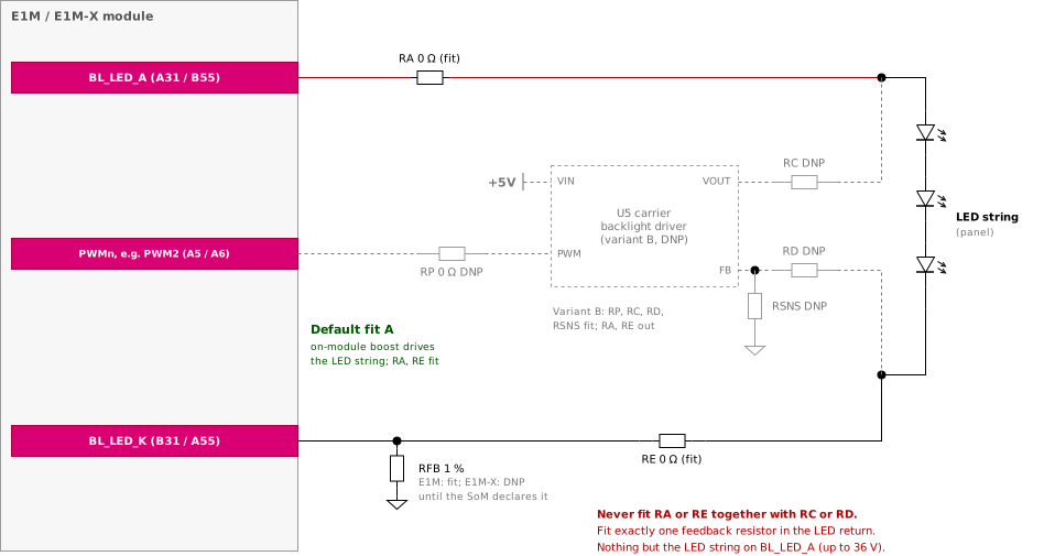
Backlight assembly options: default fit A (on-module boost on BL_LED_A through RA, LED return through RE and one RFB on BL_LED_K; RFB fitted on E1M, not fitted on E1M-X until declared) and variant B (carrier driver with PWM from a standard PWM pad through RP, output through RC, return through RD to its own sense resistor RSNS, all not fitted by default); never fit both
A panel with its own backlight driver takes its PWM input from a standard PWM pad through a translator to the panel I/O level. The E1M EVK (2641-R3) does this: the panel BL_PWM input (J6 pin 34) comes from pad A5 (PWM2 in E1M-STD §7.3.24; EVK net CK_PWM4_L) through U4 and R110 (0 Ω), and R109 (BL_LED_A to BL_PWM) is not fitted.
16.5 Parallel LCD (E1M-X)
E1M-X defines a 24-bit parallel LCD (LCD_B0–LCD_B23 on D3–AA3, LCD_HSYNC on AB3, LCD_VSYNC on AC3; E1M-STD §7.3.19). The specification gives no pixel clock and no data-enable pad, so the interface is incomplete as specified, and no current module routes it.
| ID | Strength | Rule | Source |
|---|---|---|---|
| CB-DSP-30 | MUST NOT | Route an unrelated net through the LCD pads; they keep their LCD function on other modules. | E1M-STD §7.3.4 |
| CB-DSP-31 | SHOULD NOT | Design a parallel-LCD connector on these pads until the specification defines the pixel clock and data-enable pads and a module routes them. | E1M-STD §7.3.19; Guide (informative) |
16.6 Per-module differences
| Item | E1M-AEN | E1M-X V2N | E1M-X V2N-M1 |
|---|---|---|---|
| DSI groups routed | DSI0, 2 lanes (lanes 2 / 3 and all of DSI1 not routed) | DSI0, 4 lanes (DSI1 not connected) | As V2N |
| DSI performance | 1.25 Gbps per lane, video mode only; resolution limited by link bandwidth | Up to 1920 × 1200 RGB888 @ 60 fps | As V2N |
| Backlight driver | Kinetic KTD2801ECD-TR, optional | On-module driver, optional; part not named | As V2N |
| Feedback voltage | 200 mV (KTD2801); DS-AEN-001 states 95 mV | 95 mV (DS / HG), unverified: driver part not named | 95 mV (DS), unverified: driver part not named |
| RFB location | Carrier, BL_LED_K (B31) to GND | Not stated | Not stated |
| Over-voltage threshold | 36 V | Not stated | Not stated |
| LED configuration | Up to 10 in series or 2P6S | Up to 10 in series or 2P6S | Up to 10 in series or 2P6S |
BL_PWM on BL_LED_A (module build option, not defined in E1M-STD-1.0 revision 1.4) | Assembly option, 1.8 V; not supported by this guide (CB-DSP-12) | Offered; level and frequency not stated; not supported by this guide | As V2N |
| DSI ESD on module | None | None (moved to the carrier, HG rev 0.2) | None |
| Parallel LCD | Not defined on E1M | Not connected | Not connected |
HG-V2N-001 lists two 4-lane DSI interfaces; DS-V2N-001 and the RZ/V2N have one, and the pin tables mark every DSI1 pad not connected. This guide follows the datasheet.
16.7 Chapter checklist
| Done | Check | Rule |
|---|---|---|
| ☐ | No unrelated net on a DSI or LCD pad that a module does not route. | CB-DSP-01, CB-DSP-30 |
| ☐ | DSI0 clock and four data pairs reach the connector; panel lane count suits every targeted module. | CB-DSP-02, CB-DSP-03 |
| ☐ | Pairs 100 Ω ± 10 %, matched, no swaps; TVS at the connector. | CB-DSP-05, CB-DSP-06, CB-DSP-08 |
| ☐ | Panel rails from carrier load switches that follow VIO_OUT; nothing powered from VIO_OUT directly. | CB-DSP-09 |
| ☐ | Panel control lines pulled up only to VIO_OUT on the module side; translator VCCA rated 1.65–3.6 V; reset and power held off by pull-downs. | CB-DSP-10, CB-DSP-11 |
| ☐ | Panel unpowered or in reset until firmware releases it after PORn is high. | CB-DSP-21 |
| ☐ | BL_LED_A carries only the LED anode, never a PWM or logic input; every part on it rated ≥ 40 V or the declared maximum; no TVS below the declared over-voltage. | CB-DSP-12, CB-DSP-13, CB-DSP-22 |
| ☐ | Exactly one feedback resistor; RFB sized from 200 mV on E1M-AEN; E1M-X 95 mV not relied on. | CB-DSP-14, CB-DSP-15 |
| ☐ | LED string ≤ 10 in series or 2P6S, below the over-voltage threshold (36 V on E1M-AEN); ≤ 0.8 W on E1M-AEN. | CB-DSP-17 |
| ☐ | Default fit A: RA, RE fitted; RFB fitted on E1M, not fitted on E1M-X until declared; RP, RC, RD, RSNS not fitted; never both paths. | CB-DSP-18, CB-DSP-19 |
| ☐ | Backlight input current included in the 5 V budget. | CB-DSP-20 |
17 PCIe
This chapter covers the PCIe pads, routing and AC coupling, the reference clock, the sideband signals that the specification does not define, and M.2 slots with switched slot power. E1M defines one ×4 PCIe group (PCIE0); E1M-X defines two (PCIE0, PCIE1). Of the current modules only E1M-X V2N and V2N-M1 route PCIe, and on V2N-M1 the lanes serve the on-module DX-M1 accelerator.
- A carrier clock generator driving
PCIE0_CLKwhile the module drives it puts two clock outputs on one pair (CB-PCIE-07). - M.2 sideband signals are 3.3 V; a pull-up to 3.3 V on a 1.8 V module pad exceeds its 1.98 V absolute maximum (CB-PCIE-09).
- On E1M-X V2N-M1, software outside the Alp Lab U-Boot that re-runs the DX-M1 rail sequence or writes the on-module PMIC can bring the 0.75 V DX-M1 core up at 1.80 V and damage the DX-M1 (CB-PCIE-14).
17.1 Pads
| Pair | PCIE0 E1M | PCIE0 E1M-X | PCIE1 E1M-X |
|---|---|---|---|
TX0 | A21 / B21 | A38 / B38 | A27 / B27 |
TX1 | A22 / B22 | A39 / B39 | A28 / B28 |
TX2 | A23 / B23 | A40 / B40 | A29 / B29 |
TX3 | A24 / B24 | A41 / B41 | A30 / B30 |
RX0 | A25 / B25 | A42 / B42 | A31 / B31 |
RX1 | A26 / B26 | A43 / B43 | A32 / B32 |
RX2 | A27 / B27 | A44 / B44 | A33 / B33 |
RX3 | A28 / B28 | A45 / B45 | A34 / B34 |
CLK | A29 / B29 | A47 / B47 | A36 / B36 |
TX pairs are module transmitters and connect to the receiver of the device (M.2 PERp / PERn); RX pairs connect to the device transmitter (M.2 PETp / PETn).
17.2 Routing and AC coupling
| ID | Strength | Rule | Source |
|---|---|---|---|
| CB-PCIE-01 | MUST | Treat the PCIe pads as high-speed differential pads: do not clamp, pull or level-translate them. Route them as the PCIe specifications require. | E1M-STD §6.7.1 |
| CB-PCIE-02 | SHOULD | Route each pair as 85 Ω differential and match each pair within ± 2 ps. Keep the pairs over a continuous ground plane, with ground vias beside every layer change. | HG-V2N-001 PCIe |
| CB-PCIE-03 | SHOULD | Match the lanes of one link to each other within ± 2 ps. HG-V2N-M1-001 states this lane-to-lane rule in addition to the intra-pair rule; the skew of the V2N-M1 on-module multiplexer is not yet stated. | HG-V2N-M1-001 PCIe |
| CB-PCIE-04 | MUST NOT | Route an unrelated net through a PCIe pad that a module does not route (all PCIe pads on E1M-AEN; PCIE0 lanes 2 / 3 and all of PCIE1 on V2N / V2N-M1). | E1M-STD §7.3.4, §9.2 (9) |
| CB-PCIE-05 | SHOULD | Route all four lanes of each PCIe group the carrier uses, so that a ×4 module can use them; lanes the module does not drive float. | Guide (informative) |
| CB-PCIE-06 | MUST | Put exactly one AC-coupling capacitor in series with each module TX line: 220 nF in 0201 or 0402, next to the slot, unless the SoM declares its own TX capacitors, in which case fit 0 Ω in the same footprint. For a device soldered on the carrier, also put one capacitor in each device TX line (module RX). The M.2 card carries the capacitors of its own transmitter. | HG-V2N-M1-001 PCIe; PCIe specification |
Where the AC-coupling capacitors of the module transmitter sit is not documented for E1M-X V2N or V2N-M1 (HG-V2N-M1-001 says only "AC-couple every lane"). Two capacitors in series halve the coupling capacitance; none leaves the link DC-coupled. Keep the 0201 / 0402 footprint and choose 220 nF or 0 Ω from the SoM declaration.
17.3 Reference clock
E1M-X V2N uses an on-module reference clock by default; a carrier clock is optional (HG-V2N-001). The specification does not define the direction of the PCIE0_CLK pads.
| ID | Strength | Rule | Source |
|---|---|---|---|
| CB-PCIE-07 | MUST NOT | Drive the PCIEx_CLK pads, or the slot REFCLK pair they are linked to, from a carrier clock generator unless the SoM declares the pads as a reference-clock input. Make the module clock to the slot (RE fitted) the default fit, and fit the carrier generator path (RF) only in a variant that declares such SoMs; never fit both. | HG-V2N-001 PCIe; Guide (damage) |
| CB-PCIE-08 | SHOULD | Route the reference clock as an 85 Ω pair with the same care as the data pairs, and keep it away from the data lanes and switching nodes. | HG-V2N-001 PCIe |
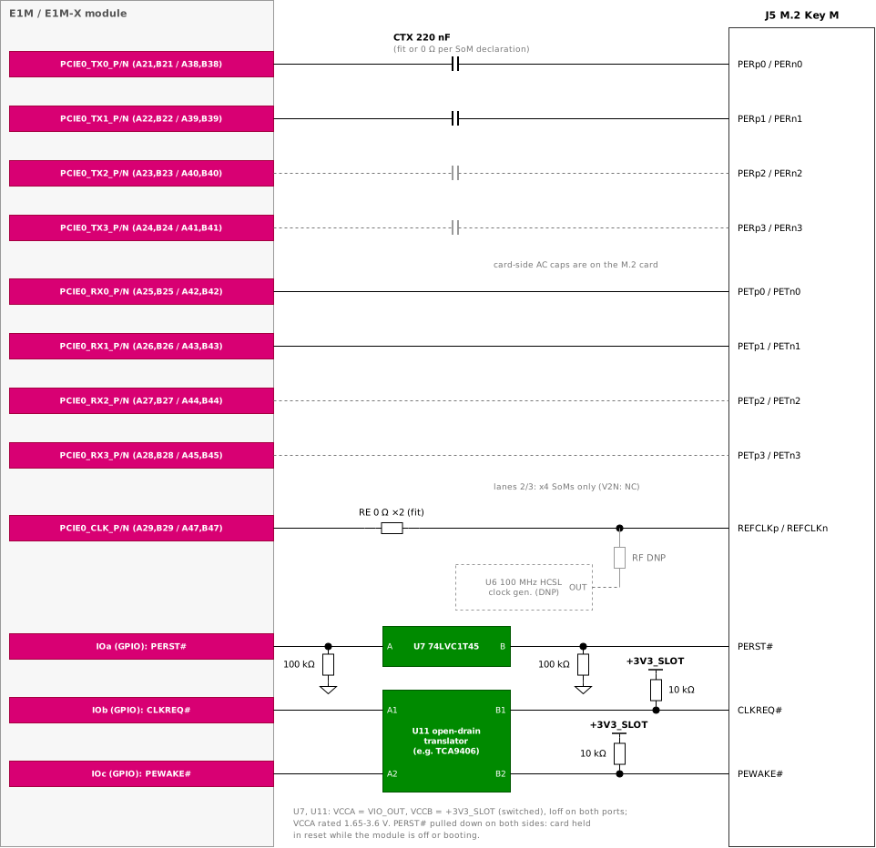
M.2 Key M reference: PCIE0 lanes with AC-coupling capacitors in the module TX lines, lanes 2 / 3 for ×4 modules, reference clock from the module (RE) with an optional carrier generator (RF, not fitted), PERST# through a fixed-direction buffer (U7) with pull-downs on both sides, and CLKREQ# / PEWAKE# through an open-drain translator (U11) with slot-side pull-ups to the switched slot rail (E1M pad / E1M-X pad)
17.4 Sideband signals
The specification has no PERST#, CLKREQ# or WAKE# pad. The carrier implements them on GPIO pads and declares the choice.
| ID | Strength | Rule | Source |
|---|---|---|---|
| CB-PCIE-09 | MUST | Translate M.2 sidebands (3.3 V) to the 1.8 V module pads with translators referenced to VIO_OUT (VCCA = VIO_OUT) whose ports are high-impedance while either supply is off (Ioff). Route PERST# (push-pull, host to card) through a fixed-direction buffer such as a 74LVC1T45-class part, or an open-drain N-MOSFET; use an open-drain-capable translator only for CLKREQ# and PEWAKE#. Fit the 3.3 V pull-ups on the slot side only; never pull a module pad above VIO_OUT. Choose translators whose VCCA is rated 1.65–3.6 V (CB-IO-22, informative). | E1M-STD §6.2.3 (4), (5), §6.1.2 (5) |
| CB-PCIE-10 | MUST | Where a sideband uses a function beyond the pad's default and GPIO secondary (for example a hardware PERST# output of the SoC), declare it as a per-SoM dependency and reject SoMs that do not expose it. | E1M-STD §8.4, §9.2 (2) |
| CB-PCIE-11 | SHOULD | Use SoC-owned GPIOs and record the assignment in the carrier build files. Avoid E1M-AEN IO13, IO15–IO24 (not SoC GPIOs) and E1M-X V2N-M1 IO0–IO6, IO17–IO22, IO24 (routed to the DX-M1). | DS-AEN-001; DS-V2N-M1-001 |
| CB-PCIE-12 | SHOULD | Hold PERST# asserted by default with 100 kΩ pull-downs on both sides of its buffer, so the card stays in reset while the module is off or booting. Do not route PERST# through an auto-direction translator: its integrated pull-ups (about 10 kΩ) override the pull-downs and release the card while the module GPIO is still an input. | E1M-STD §6.2.3 (1); Guide (informative) |
| CB-PCIE-17 | SHOULD | Reference the slot-side sideband pull-ups and the translator VCCB to the switched slot 3.3 V rail, not to an always-on rail, so that no current flows into an unpowered card. | Guide (informative) |
17.5 M.2 slots and slot power
| ID | Strength | Rule | Source |
|---|---|---|---|
| CB-PCIE-13 | SHOULD | Supply the 3.3 V slot rail through a load switch with soft-start, enabled by a GPIO with a pull-down so the slot is off by default. Enable it only when the SoM routes the PCIe group to the carrier; on E1M-AEN the slot stays off. | Guide (informative) |
| CB-PCIE-14 | MUST NOT | On E1M-X V2N-M1, re-run the DX-M1 rail sequence, drive the DX-M1 rail enable or write the on-module PMIC outside the Alp Lab U-Boot (from carrier software, a Cortex-M33 image, a Linux application or a bench tool). A replacement boot loader MUST implement the complete sequence in the documented order: rail on and confirmed good, then reset release and PCIe multiplexer routing. On V2N-M1 a carrier device on PCIE0 is not reachable with the stock image. | HG-V2N-M1-001 Boot, PCIe |
| CB-PCIE-15 | SHOULD | Size the 5 V source for PCIe loads: E1M-X V2N / V2N-M1 recommend a 5 V source ≥ 5 A peak to cover AI load, two Ethernet ports and an M.2 SSD. Include the slot 3.3 V converter losses. | HG-V2N-001; DS-V2N-001 |
| CB-PCIE-16 | MAY | Share one PCIe group between two M.2 slots (for example Key M and Key E) through PCIe lane switches and a 1:2 reference-clock buffer, one slot active at a time, with sidebands and slot power switched per slot. | Guide (informative); topology of the E1M EVK footprint (lane switches U42, U43, U50, U51, clock buffer U44; not fitted on E1M-AEN); E1M-X EVK scheme TBD (UG-E1M-X-001) |
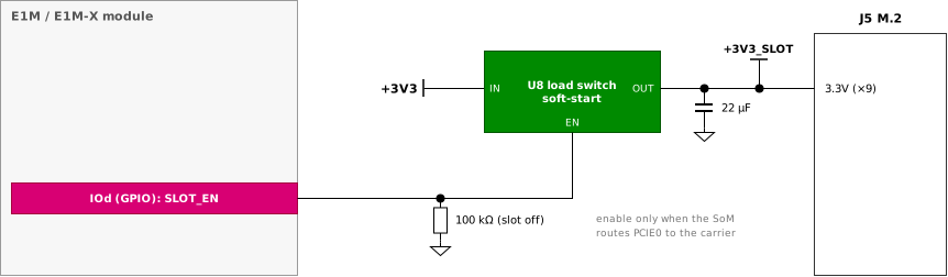
M.2 slot power: 3.3 V through a soft-start load switch to the switched slot rail +3V3_SLOT, enabled by a GPIO with a pull-down so the slot is off by default
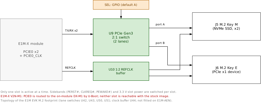
Sharing PCIE0 between an M.2 Key M and a Key E slot with a 2:1 PCIe switch and a 1:2 reference-clock buffer (block diagram; topology of the E1M EVK footprint, not fitted on E1M-AEN; the E1M-X EVK scheme is TBD)
17.6 Per-module differences
| Item | E1M-AEN | E1M-X V2N | E1M-X V2N-M1 |
|---|---|---|---|
| PCIe routed | None; leave all PCIE0 pads floating | PCIE0 Gen3 ×2 (lanes 0 / 1); lanes 2 / 3 and PCIE1 not connected | PCIE0 Gen3 ×2, multiplexed with the on-module DX-M1 |
Carrier device on PCIE0 | — | Reachable | Not reachable with the stock image (U-Boot routes the lanes to the DX-M1 on every boot; no API to switch) |
| Reference clock | — | On-module clock by default; carrier clock optional; pad direction not stated | As V2N |
| Skew rules | — | 85 Ω; ± 2 ps within each pair | 85 Ω; ± 2 ps lane to lane; multiplexer skew not stated |
| AC-coupling location | — | Not stated | "AC-couple every lane"; location not stated |
| Sideband pads | — | None defined; GPIO | None defined; GPIO (avoid DX-M1-owned IO0–IO6, IO17–IO22, IO24) |
17.7 Chapter checklist
| Done | Check | Rule |
|---|---|---|
| ☐ | Pairs 85 Ω, ± 2 ps within each pair and lane to lane; no clamps or pulls. | CB-PCIE-01 to CB-PCIE-03 |
| ☐ | No unrelated net on a PCIe pad that a module does not route. | CB-PCIE-04 |
| ☐ | Exactly one AC-coupling capacitor (or 0 Ω per SoM) in each module TX line. | CB-PCIE-06 |
| ☐ | Module reference clock is the default; carrier generator not fitted unless declared; never both. | CB-PCIE-07 |
| ☐ | Sidebands translated to VIO_OUT (VCCA rated 1.65–3.6 V, Ioff); PERST# through a fixed-direction buffer with pull-downs on both sides; 3.3 V pull-ups on the slot side only, to the switched slot rail. | CB-PCIE-09, CB-PCIE-12, CB-PCIE-17 |
| ☐ | Sideband GPIOs SoC-owned and declared; tertiary functions declared as per-SoM dependencies. | CB-PCIE-10, CB-PCIE-11 |
| ☐ | Slot 3.3 V switched, off by default, enabled only for SoMs that route PCIe. | CB-PCIE-13 |
| ☐ | V2N-M1: carrier PCIe device not expected to work; nothing outside the Alp Lab U-Boot (or a replacement that implements the full sequence) touches the DX-M1 rails or PMIC. | CB-PCIE-14 |
| ☐ | 5 V source sized for PCIe and AI load. | CB-PCIE-15 |
18 CAN
A CAN group (CAN0, and on E1M-X also CAN1) reaches the carrier in one of two options, and the SoM declares the option for each group in its manifest (E1M-STD §6.5). The same pads then carry either bus-level signals or 1.8 V logic signals. This chapter gives one carrier circuit that accepts both, and the termination, protection, CAN_STBY and isolation rules around it.
18.1 Pads
| Pad | E1M | E1M-X | Reading (fixed by the declared CAN option) |
|---|---|---|---|
CAN0H/CAN0_TX | B18 | B21 | Bus-level: CAN0H. Logic-level: CAN0_TX, SoM output, VIO_OUT domain. |
CAN0L/CAN0_RX | B19 | B22 | Bus-level: CAN0L. Logic-level: CAN0_RX, SoM input, VIO_OUT domain. |
CAN1H/CAN1_TX | — | B24 | As CAN0H/CAN0_TX (E1M-X only). |
CAN1L/CAN1_RX | — | B25 | As CAN0L/CAN0_RX (E1M-X only). |
CAN_STBY | A19 | A21 | Standby control of the transceiver. Direction and polarity are declared per SoM (E1M-STD §7.3.14). |
E1M pad A19 is CAN_STBY, but E1M-X pad A19 is DAC0; never carry a CAN net assignment from one form factor to the other by pad ID.
18.2 CAN options in the specification
| Option | Pads carry | Transceiver | Carrier provides |
|---|---|---|---|
| Bus-level CAN (default) | CANxH, CANxL from the on-module transceiver | On the SoM. The carrier SHALL NOT add one. | Termination, bus-side ESD protection, connector. |
| Logic-level CAN (declared option) | CANx_TX (SoM output), CANx_RX (SoM input), 1.8 V VIO_OUT domain | On the carrier. The carrier SHALL provide it. | Transceiver, termination, bus-side ESD protection, connector. |
The reading of a compound CAN pad is not a carrier choice: the carrier uses the reading that the SoM declares for that group (E1M-STD §8.3). A carrier that accepts both options therefore needs two assembly variants of the CAN path (E1M-STD §6.7.2).
A CAN bus, terminator or bus-side protection connected straight to logic-level CAN pads destroys the SoC, because on the E1M-AEN standard build B18 / B19 are 1.8 V SoC pads with an absolute maximum of − 0.3 V to 1.98 V.
| ID | Strength | Rule | Source |
|---|---|---|---|
| CB-CAN-01 | MUST NOT | Connect a CAN bus, a bus terminator or bus-side protection directly to a CAN pad, unless every SoM that the build variant declares support for implements that CAN group as bus-level CAN. | E1M-STD §7.3.14; DS-AEN-001 CAN Bus |
| CB-CAN-02 | MUST | Use, for each CAN group, the reading the SoM declares (bus-level CANxH / CANxL or logic-level CANx_TX / CANx_RX). | E1M-STD §8.3, §7.3.14 |
| CB-CAN-03 | MUST | Make the carrier-transceiver path the default assembly of every CAN group (the fit used when no SoM set is declared), with the bypass path not fitted. | E1M-STD §6.7.2 (1), (2) |
| CB-CAN-04 | MUST NOT | Fit the carrier-transceiver path and the bypass path of the same CAN group at the same time. | E1M-STD §6.7.2 (4) |
| CB-CAN-05 | MUST | Fit the bypass path (transceiver out of circuit) only in a build variant that declares a SoM set in which every SoM declares bus-level CAN for the groups concerned. | E1M-STD §6.7.2 (3) |
| CB-CAN-06 | MUST | Declare, for every build variant, the fit of each CAN group and the SoMs the variant supports. | E1M-STD §6.7.2 (5), §9.2 (8) |
| CB-CAN-07 | MUST NOT | Add a CAN transceiver in the path of a group that the SoM declares bus-level. The bypass variant meets this rule: the carrier transceiver is disconnected from the pads and from the bus. | E1M-STD §6.5, §7.3.14 |
18.3 Dual-build carrier circuit
The circuit below is the carrier half of both options. In the default fit the carrier transceiver U1 sits between the CAN pads and the bus. This is correct for a logic-level SoM. With a bus-level SoM on the default fit, CAN does not work until the bypass variant is fitted (E1M-STD §6.7.2 (3)). The SoM's bus pins then see only U1 TXD and RXD, so the voltages on U1 stay within what the SoM transceiver drives (about 0–5 V). The TCAN1044AV-Q1 rates its logic inputs TXD / STB and its RXD pin at − 0.3 V to 6 V against GND, independent of VIO, with ≤ 1 μA leakage at 5.5 V while VCC = VIO = 0 V (TI SLLSFJ3D, §6.1 and §6.5), so the SoM's CANH on TXD does not inject current into +1V8_SW. But RXD is a push-pull output that then drives against the SoM's CANL driver, and nothing in the circuit limits that current to the RXD rating of ± 8 mA. Whether U1 survives is not verified (CB-CAN-27). The bypass variant takes U1 out of the path with four 0 Ω links and connects the pads straight to the bus side through two other links.
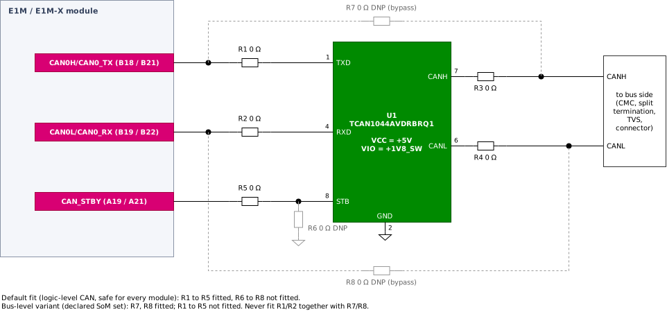
Dual-build CAN path for one CAN group: carrier transceiver U1 (default fit) and the not-fitted bypass R7 / R8 for a bus-level SoM. Pads shown as E1M / E1M-X; CAN1 on E1M-X uses B24 / B25 with its own copy of the circuit
| Part | Function | Default fit (logic-level SoM) | Bus-level variant | E1M EVK 2641-R3 |
|---|---|---|---|---|
U1 | TCAN1044AVDRBRQ1, VCC = +5V, VIO = +1V8_SW | fitted | may stay fitted, disconnected | U6 |
R1 | 0 Ω, pad CAN0H/CAN0_TX to U1 TXD (pin 1) | fitted | not fitted | R34 |
R2 | 0 Ω, U1 RXD (pin 4) to pad CAN0L/CAN0_RX | fitted | not fitted | R246 |
R3 | 0 Ω, U1 CANH (pin 7) to the bus side | fitted | not fitted | R247 |
R4 | 0 Ω, U1 CANL (pin 6) to the bus side | fitted | not fitted | R248 |
R5 | 0 Ω, pad CAN_STBY to U1 STB (pin 8) | fitted | not fitted | none (direct) |
R6 | 0 Ω, U1 STB to GND (permanent normal mode) | not fitted | not fitted | none |
R7 | 0 Ω bypass, pad CAN0H/CAN0_TX to bus CANH | not fitted | fitted | R249 |
R8 | 0 Ω bypass, pad CAN0L/CAN0_RX to bus CANL | not fitted | fitted | R250 |
+1V8_SW is a carrier 1.8 V rail switched by VIO_OUT (E1M-STD §6.1.2 (3), use (c)); see Chapter 6. The E1M EVK 2641-R3 builds this path with U6 fitted and the bypass R249 / R250 not fitted, and documents the rework for a SoM with an on-module CAN PHY: remove R34, R246, R247 and R248, then fit R249 and R250.
| ID | Strength | Rule | Source |
|---|---|---|---|
| CB-CAN-08 | MUST | Supply the logic side (VIO) of the carrier transceiver from VIO_OUT or from a carrier rail switched by VIO_OUT, and use a transceiver whose logic pins stay high-impedance while it is unpowered (TCAN1044AV-Q1: ≤ 1 μA at 5.5 V with VCC = VIO = 0 V). | E1M-STD §7.3.14, §6.2.3 (1); TI SLLSFJ3D §6.5 |
| CB-CAN-09 | MUST | Choose a transceiver whose VIO range includes 1.71 V (VIO_OUT 1.8 V − 5 %; TCAN1044AV-Q1: 1.7–5.5 V), and whose logic-pin absolute maximum, referred to GND and valid with VIO at 0 V, covers the dominant and recessive levels a bus-level SoM can put on TXD, RXD and STB (TCAN1044AV-Q1: − 0.3 V to 6 V). | E1M-STD §6.1.2 (1), §6.7.2 (1); TI SLLSFJ3D §6.1, §6.4 |
| CB-CAN-10 | SHOULD | Use TCAN1044AVDRBRQ1: it is the transceiver of the E1M-X V2N family, of the E1M-AEN transceiver option and of the E1M EVK. | HG-V2N-001 CAN; DS-AEN-001 CAN Bus; UG-E1M-001 CAN Bus |
| CB-CAN-11 | SHOULD | Place the 0 Ω links of both paths next to the transceiver, so that the unused stubs are short in both variants. | Guide (informative) |
| CB-CAN-27 | SHOULD NOT | Operate a bus-level SoM on the default fit beyond a first power-up check: CAN does not work, and the carrier transceiver RXD output then drives against the SoM's CANL driver with no current limit. Fit the bypass variant first. | E1M-STD §6.7.2 (3); TI SLLSFJ3D §6.1; Guide (informative) |
18.4 Termination, protection and routing
The bus side is the same for both variants. It starts at the node where R3 / R7 and R4 / R8 meet.
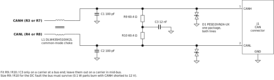
Bus side of a CAN group: common-mode choke L1, line capacitors, split termination R9 / R10 / C3, TVS D1 and connector J1 (values from the E1M EVK 2641-R3)
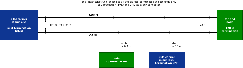
CAN bus topology: one linear bus, 120 Ω at both ends only, short stubs
| ID | Strength | Rule | Source |
|---|---|---|---|
| CB-CAN-12 | MUST | Provide, for every CAN group the carrier uses and in both variants, the termination footprint (fitted when the carrier sits at a bus end, CB-CAN-14), bus-side ESD protection and the connector. | E1M-STD §6.5, §7.3.14; HG-V2N-001 CAN |
| CB-CAN-13 | SHOULD | Terminate with a split 120 Ω network: 2 × 60.4 Ω in series between CANH and CANL, with the centre tap to GND through a capacitor (12 nF on the E1M EVK). | UG-E1M-001 CAN Bus |
| CB-CAN-14 | SHOULD | Fit the termination only on a carrier that sits at a bus end, and make it a not-fitted option or a jumper on a carrier that can sit mid-bus. With the bus unpowered, CANH to CANL measures about 60 Ω when exactly two terminators are fitted. | AN-005; Guide (informative) |
| CB-CAN-15 | SHOULD | Rate the termination resistors for the DC fault the product must survive. On the E1M EVK, 0.1 W parts take about 0.6 W each with CANH shorted to 12 V and burn. | UG-E1M-001 CAN Bus |
| CB-CAN-16 | SHOULD | Fit a common-mode choke (DLW43SH510XK2L) between the transceiver / bypass node and the connector, 100 pF from each line to GND on the connector side, and a CAN TVS (PESD2IVN24-UX) next to the connector. | DS-AEN-001 CAN Bus; UG-E1M-001 CAN Bus |
| CB-CAN-17 | SHOULD | Route CANH / CANL as a coupled pair over a continuous ground plane, and keep the stub from the bus to each node short (≤ 0.3 m is the usual limit at 1 Mbit/s; shorter at CAN FD data rates). | Guide (informative) |
18.5 CAN_STBY
CAN_STBY means different things on different builds. On the E1M-AEN standard build it is a SoC GPIO, which firmware can use to drive the STB input of the carrier transceiver. On the E1M-AEN transceiver option it is the standby input of the on-module transceiver (low = normal mode, several mA). On E1M-X V2N / V2N-M1 its direction is not yet documented. The circuit above therefore connects it through a removable link and never pulls it low. The only pull on it is the weak internal STB pull-up of the carrier transceiver to its VIO rail, which is switched by VIO_OUT and therefore allowed (E1M-STD §6.2.3 (4)).
CAN_STBY rules| ID | Strength | Rule | Source |
|---|---|---|---|
| CB-CAN-18 | MUST NOT | Pull CAN_STBY (E1M A19 / E1M-X A21) low. | E1M-STD §7.3.14; DS-AEN-001 CAN Bus |
| CB-CAN-19 | MUST NOT | Drive CAN_STBY from a carrier circuit unless the SoM manifest declares it a SoM input. | E1M-STD §7.3.14 |
| CB-CAN-20 | SHOULD | In the default fit, connect CAN_STBY to the carrier transceiver STB through R5, without a carrier pull resistor. The internal STB pull-up of TCAN1044AVDRBRQ1 keeps the transceiver in standby until the SoM drives CAN_STBY low for normal mode. | UG-E1M-001 CAN Bus |
| CB-CAN-21 | MAY | For a logic-level SoM that does not use CAN_STBY, remove R5 and fit R6, so that the carrier transceiver stays in normal mode. | Guide (informative) |
| CB-CAN-22 | MUST NOT | Fit R5 and R6 together: that pulls CAN_STBY low. | E1M-STD §7.3.14 |
| CB-CAN-23 | SHOULD | Leave R5 not fitted in the bus-level variant, so that the disconnected carrier transceiver does not load CAN_STBY. | Guide (informative) |
18.6 Isolation
A bus-level SoM has its transceiver on the module, referenced to the module GND, and the carrier may not add a second transceiver (CB-CAN-07). A carrier therefore cannot galvanically isolate such a bus. Isolation is possible only for logic-level groups: replace U1 with an isolated CAN transceiver and feed its bus side from an isolated DC/DC converter.
| ID | Strength | Rule | Source |
|---|---|---|---|
| CB-CAN-24 | MUST | Declare, for an isolated CAN design, a SoM set in which every SoM declares logic-level CAN for the isolated groups. Such a carrier has no bypass variant. | E1M-STD §6.5, §6.7.2 (5) |
| CB-CAN-25 | MUST | Supply the logic side of an isolated transceiver from a carrier rail switched by VIO_OUT, with a logic-side range that includes 1.71 V and logic pins that stay high-impedance while unpowered. | E1M-STD §7.3.14, §6.1.2 (1) |
| CB-CAN-26 | SHOULD | Keep the creepage and clearance distances of the isolation barrier free of copper, including the ground planes of both sides. | Guide (informative) |
18.7 Per-module differences
| Item | E1M-AEN | E1M-X V2N | E1M-X V2N-M1 |
|---|---|---|---|
| CAN groups | CAN0 only | CAN0, CAN1 | As V2N |
| Standard build | Logic-level CAN, declared in the manifest: no on-module transceiver; B18 = CAN0_TX, B19 = CAN0_RX, 1.8 V SoC logic | Bus-level CAN: 2 × TCAN1044AVDRBRQ1 on the module, populated by default (HG-V2N-001); DS-V2N-001 calls them optional | As V2N |
| Other build | Assembly option with on-module TCAN1044AVDRBRQ1: B18 = CAN0H, B19 = CAN0L (bus-level); contact Alp Lab | A build without transceivers is not documented | As V2N |
| CAN pad absolute maximum | Standard build: − 0.3 V to 1.98 V. Transceiver option: − 58 V to +58 V | Not stated in the module documents | As V2N |
CAN_STBY | A19. Standard build: SoC GPIO. Transceiver option: transceiver standby input, low = normal mode; never pull it low | A21, "standby control"; direction and polarity TBD | As V2N |
| Carrier fit to use | Default fit (carrier transceiver) | Bus-level variant (bypass) | Bus-level variant (bypass) |
| CAN controller | Alif Ensemble | RZ/V2N CAN FD; 2 groups on pads | As V2N |
18.8 Chapter checklist
| ID | Check | Done |
|---|---|---|
| CB-CAN-01 | No CAN pad connects straight to a bus, terminator or TVS in the default fit. | ☐ |
| CB-CAN-03, 04 | The default fit is the carrier-transceiver path, the bypass links are not fitted, and the two paths of a group are never both fitted. | ☐ |
| CB-CAN-05, 06 | Every build variant states its CAN fit and its supported SoM set. | ☐ |
| CB-CAN-08, 09 | Transceiver VIO from a VIO_OUT-switched rail, VIO range includes 1.71 V, logic pins high-impedance while unpowered and rated for bus-level SoM voltages. | ☐ |
| CB-CAN-27 | A bus-level SoM is run only on the bypass variant. | ☐ |
| CB-CAN-12, 13, 14 | Termination footprint, ESD protection and connector present; termination fitted only at a bus end; about 60 Ω across the unpowered bus. | ☐ |
| CB-CAN-15 | Termination resistors rated for the DC bus fault. | ☐ |
| CB-CAN-16, 17 | Choke, line capacitors and TVS at the connector; pair routed coupled; stubs short. | ☐ |
| CB-CAN-18, 19, 22 | CAN_STBY never pulled low or driven by the carrier; R5 and R6 never fitted together. | ☐ |
| CB-CAN-24, 25 | An isolated design declares a logic-level-only SoM set and powers the isolator logic side from a VIO_OUT-switched rail. | ☐ |
19 I2C, I3C, UART, SPI, I2S and PDM
Every pad in this chapter is in the VIO_OUT (1.8 V) domain (E1M-STD §6.7.1), so the back-powering and I/O-gating rules of Chapter 7 apply to all of them: drive only while VIO_OUT and PORn are high, pull up only to VIO_OUT or a rail it switches, and stay between − 0.3 V and 1.98 V (E1M-STD §6.2.3). The rules below add what is specific to each bus.
19.1 Pads
| Interface | E1M | E1M-X |
|---|---|---|
I2C0 | I2C0_SCL AE2, I2C0_SDA AD2 | I2C0_SCL AH1, I2C0_SDA AH2 |
I2C1 | I2C1_SCL AG17, I2C1_SDA AH17 | I2C1_SCL AQ47, I2C1_SDA AR47 |
I2C2, I2C3 | — | I2C2_SCL E64, I2C2_SDA E63; I2C3_SCL A24, I2C3_SDA A23 |
I3C | I3C_SCL AG5, I3C_SDA AH5 | I3C_SCL AQ19, I3C_SDA AR19 |
UART0 | UART0_TX F2, UART0_RX G2 | UART0_TX AA2, UART0_RX AB2 |
UART1 | UART1_TX AG4, UART1_RX AH4 | UART1_TX AQ17, UART1_RX AR17 |
| Debug console | DBG_TX AD3, DBG_RX AE3 | DBG_TX AC62, DBG_RX AD62 |
SPI0 | SPI0_SCLK N2, SPI0_MOSI M2, SPI0_MISO L1, SPI0_CS0 M1, SPI0_CS1 N1 | SPI0_SCLK AE2, SPI0_MOSI AD2, SPI0_MISO AD1, SPI0_CS0 AE1, SPI0_CS1 AF1 |
SPI1 | SPI1_SCLK AG10, SPI1_MOSI AG9, SPI1_MISO AG8, SPI1_CS0 AH9, SPI1_CS1 AH8 | SPI1_SCLK AR15, SPI1_MOSI AQ14, SPI1_MISO AQ13, SPI1_CS0 AR14, SPI1_CS1 AR13 |
SPI2 | — | SPI2_SCLK C63, SPI2_MOSI B64, SPI2_MISO B63, SPI2_CS0 C64, SPI2_CS1 D64 |
I2S0 | I2S0_SCLK AE33, I2S0_WS AE34, I2S0_SDO AD34, I2S0_SDI AD33 | I2S0_SCLK AQ5, I2S0_WS AR5, I2S0_SDO AR4, I2S0_SDI AQ4 |
I2S1 | I2S1_SCLK AH7, I2S1_WS AG7, I2S1_SDO AG6, I2S1_SDI AH6 | I2S1_SCLK AR11, I2S1_WS AQ11, I2S1_SDO AQ10, I2S1_SDI AR10 |
| Audio master clock | AUDIO_CLK Z2 | AUDIO_CLK AR9 |
PDM0 | PDM_C0 AA1, PDM_D0 AA2 | PDM_C0 AQ7, PDM_D0 AR7 |
PDM1 | PDM_C1 AB1, PDM_D1 AB2 | PDM_C1 AQ8, PDM_D1 AR8 |
A microphone clock routed to E1M-X AA1 switches the module off, so never carry a net assignment from one form factor to the other by pad ID.
| Pad | E1M | E1M-X | Effect of a net carried by pad ID |
|---|---|---|---|
AA1, AB1 | PDM_C0, PDM_C1 | MODULE_EN, MODULE_STBY | A microphone clock or its pull switches an E1M-X module off or into standby. |
AA2, AB2 | PDM_D0, PDM_D1 | UART0_TX, UART0_RX | A microphone data output on AA2 contends with the E1M-X UART0_TX output. |
AE2 | I2C0_SCL | SPI0_SCLK | An I2C pull-up and devices load an SPI clock output. |
AH1 | ANT_2.4GHZ | I2C0_SCL | An RF feed or matching network lands on an I2C line, or an I2C bus on the antenna port. |
AF1, AD1 | ANT_5GHZ, ANT_6GHZ | SPI0_CS1, SPI0_MISO | As above, for SPI. |
19.2 I2C and I3C
19.2.1 Pull-ups and bus loading
None of the three reference modules has documented pull-ups on its I2C or I3C pads, and the module datasheets require external pull-ups, so the carrier fits them. The pull-up value follows from the bus capacitance Cb and the rise time tr of the speed mode (UM10204):
Rp(max) = tr / (0.8473 ⋅ Cb)
Rp(min) = (VVIO,max − VOL) / IOL = (1.89 V − 0.378 V) / (3 mA) ≈ 504 Ω
with VOL = 0.2 ⋅ VVIO for supplies below 2 V, taken at the same supply corner (0.2 × 1.89 V = 0.378 V). With 4.7 kΩ the bus supports about 250 pF in Standard-mode (tr = 1000 ns) and about 75 pF in Fast-mode (tr = 300 ns). With 2.2 kΩ the limits are 400 pF and about 160 pF.
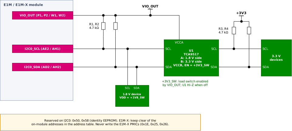
I2C0 reference: pull-ups to VIO_OUT, a 1.8 V device on a VIO_OUT-switched rail, and a buffer U1 (TCA9517, A side VCCA = VIO_OUT, B side and EN on a VIO_OUT-switched 3.3 V rail) to 3.3 V devices
| ID | Strength | Rule | Source |
|---|---|---|---|
| CB-SER-01 | MUST | Pull I2C and I3C pads up only to VIO_OUT or to a carrier rail switched by VIO_OUT; never to 3.3 V or to an always-on rail. | E1M-STD §6.2.3 (4); HG-AEN-001 Interfaces |
| CB-SER-02 | SHOULD | Fit pull-ups on every I2C bus the carrier uses: 4.7 kΩ by default, 2.2 kΩ where the bus capacitance needs it, and never below about 510 Ω in total (504 Ω rounded up) (all pull-ups in parallel). | DS-AEN-001 I2C; DS-V2N-001 I2C; UM10204 |
| CB-SER-03 | SHOULD | Keep the bus capacitance at or below 400 pF, and size Rp for the rise time of the speed mode in use. | HG-AEN-001 Interfaces; UM10204 |
| CB-SER-04 | MUST | Connect to the 1.8 V bus only devices that are unpowered whenever VIO_OUT is low (supply from a VIO_OUT-switched rail). A device on an always-on rail drives or clamps the bus into an unpowered SoM. | E1M-STD §6.2.3 (1) |
| CB-SER-05 | MUST | Connect devices on other supplies (3.3 V, always-on) through an I2C translator or buffer referenced to VIO_OUT whose ports are high-impedance while its VIO_OUT-side supply is off. Use the datasheet to confirm it: TCA9517 states high-impedance I2C pins and 5.5 V tolerance only for the powered-off device (VCCA and/or VCCB = 0 V), so power its B side (VCCB) from a 3.3 V rail switched by VIO_OUT (figure); the 3.3 V devices may stay always-on. | E1M-STD §6.1.2 (5); TI SCPS242D §1, §9.1 |
| CB-SER-06 | SHOULD | Choose I2C translators whose VIO_OUT-side supply is rated 1.65–3.6 V (TCA9517 A side: 0.9–5.5 V), put their hard-low side on the 1.8 V bus (TCA9517: A side; its B side has the 0.5 V buffered low and never joins another B side or a static-offset device), and check which supply the EN threshold refers to before driving it. | E1M-STD §6.1.2 (informative note); TI SCPS242D §5, §7.3 |
| CB-SER-28 | MUST NOT | Tie a translator EN input to VIO_OUT unless its threshold refers to the VIO_OUT-side supply and it has no internal pull-up to another rail. TCA9517 EN has VIH = 0.7 ⋅ VCCB (2.31 V at 3.3 V, not met by 1.71 V) and an internal pull-up to VCCB, which would back-feed VIO_OUT. | E1M-STD §6.1.2 (2); TI SCPS242D §7.3, §9.3.2 |
| CB-SER-07 | SHOULD | Fit pull-up footprints from I3C_SCL and I3C_SDA to VIO_OUT; the value is TBD for all three modules. Put legacy I2C devices on the I3C bus only if they have the 50 ns spike filter that mixed I3C buses need. | DS-AEN-001 I3C; DS-V2N-001 I3C; MIPI I3C (informative) |
19.2.2 Reserved addresses
The identity EEPROM N24S128C4DYT3G of every reference module answers on I2C0 at two addresses: 0x50 (array) and 0x58 (Secure Data Page with the unique ID). On E1M-X the modules carry more I2C devices on an on-module board bus. Whether that bus reaches any E1M-X pad is not documented, so an any-module carrier keeps all of them clear.
| Address | Device | Modules | Bus as documented |
|---|---|---|---|
0x50, 0x58 | N24S128C4DYT3G identity EEPROM | E1M-AEN, V2N, V2N-M1 | I2C0. HG-V2N-001 calls it optional; DS-V2N-001 lists it in every configuration. |
0x1E | DA9292 PMIC | V2N, V2N-M1 | On-module board bus; exposure on pads not confirmed. |
0x25, 0x26 | ACT88760 PMIC | V2N, V2N-M1 | As above. |
0x30 | OPTIGA Trust M | V2N, V2N-M1 | As above. |
0x40 | TMP112 temperature sensor (TMP112DIDPWR, ADD0 = GND) | V2N, V2N-M1 | As above. AN-001 rev 0.4 and the Alp SDK chip manifest (measured) give 0x40; AN-001 rev 0.3 gave 0x48. Keep both clear. |
0x52 | RV-3028-C7 RTC | V2N, V2N-M1 | As above. On E1M-AEN the RTC is on the private bus of the RSVD pads U3 / V3. |
0x69 | 5L35023B clock generator | V2N, V2N-M1 | As above. |
0x70 | GD32G553 I/O MCU bridge | V2N, V2N-M1 | As above. |
0x4D | TPS628640 (optional) | V2N, V2N-M1 | As above. |
0x44, 0x48, 0x4F | TPS628640 DX-M1 rails | V2N-M1 | As above. The 0x48 instance answers only after the DX-M1 rail bring-up (AN-009). |
On E1M-X V2N-M1 any second writer to the on-module PMIC can bring the 0.75 V DX-M1 core rail up at the PMIC's 1.80 V default, which can damage the DX-M1.
| ID | Strength | Rule | Source |
|---|---|---|---|
| CB-SER-08 | MUST NOT | Place a carrier device at 0x50 or 0x58 on I2C0; a write to a colliding address can overwrite the module identity. | DS-AEN-001 I2C; DS-V2N-001; AN-001 |
| CB-SER-09 | MUST NOT | Fit a second I2C controller (a carrier MCU, BMC or test header used as a controller) on an E1M-X I2C bus, or address 0x1E, 0x25 or 0x26 from it, unless the SoM manifest states that the bus does not reach the on-module PMICs. This is a provisional guide precaution until the SoM manifest publishes the bus map: the hazard is a second writer to the PMIC, and which bus the PMIC sits on is not documented. | HG-V2N-M1-001 Power; AN-001; Guide (provisional) |
| CB-SER-29 | MUST NOT | Fit any carrier I2C controller on E1M-X I2C3 (A24 / A23): it is the bus of the GD32G553 I/O MCU, reached through the module bridge firmware, which owns its timing and the controller role. Carrier target devices on I2C3 are not documented; avoid them until the SoM manifest allows them. | DS-V2N-001; Guide (provisional) |
| CB-SER-10 | SHOULD | Keep carrier devices on every E1M-X I2C bus clear of all addresses in the table above until the SoM manifest states which bus carries them; watch broadcast addresses too (for example the TAS2563 global address 0x48). | E1M-STD Annex A.2; AN-001; Guide (informative) |
19.3 UART
Only TX and RX are defined for each UART. TX is a SoM output and RX a SoM input. The debug console DBG_TX / DBG_RX is covered in Chapter 9.
| ID | Strength | Rule | Source |
|---|---|---|---|
| CB-SER-11 | MUST | Drive UARTx_RX only while VIO_OUT and PORn are high. A USB-to-UART bridge, RS-232 or RS-485 transceiver on the pads has its logic side referenced to VIO_OUT and keeps its outputs high-impedance while VIO_OUT is low. | E1M-STD §6.2.3 (1), (3) |
| CB-SER-12 | MUST NOT | Rely on RTS / CTS flow control unless the carrier declares a per-SoM dependency on that tertiary function and rejects SoMs whose manifest does not expose it. | E1M-STD §7.3.10, §8.4 |
| CB-SER-13 | MAY | Fit a weak pull-up (≥ 100 kΩ) from UARTx_RX to VIO_OUT, so that the line idles high while the carrier transceiver is high-impedance. | Guide (informative) |
19.4 SPI
| ID | Strength | Rule | Source |
|---|---|---|---|
| CB-SER-14 | MUST | On E1M, never drive or pull up the SPI1 pads (AG8, AG9, AG10, AH8, AH9) while the module's radio supply is off: on E1M-AEN they are the SPI of the on-module Wi-Fi module, powered only while Wi-Fi is on, also while VIO_OUT is high. | E1M-STD §6.2.3 (7); DS-AEN-001 Pin Description |
| CB-SER-15 | SHOULD | On E1M, put carrier SPI devices on SPI0. Use SPI1 only in a build variant whose declared SoM set excludes E1M-AEN. | HG-AEN-001 Interfaces; Guide (informative) |
| CB-SER-16 | SHOULD | Use the CS0 / CS1 pads of each instance. An extra chip select from a GPIO pad must be SoC-owned on every module in the declared set (Chapter 20). | E1M-STD §7.3.11; Guide (informative) |
| CB-SER-17 | MUST | Supply SPI peripherals from a VIO_OUT-switched rail or buffer their MISO, so that no peripheral drives MISO into an unpowered SoM. | E1M-STD §6.2.3 (1) |
| CB-SER-18 | SHOULD | Pull each chip select up to VIO_OUT (for example 100 kΩ) so that peripherals stay deselected while the SoM boots; not on the E1M SPI1 pads (CB-SER-14). | Guide (informative) |
| CB-SER-19 | SHOULD | Place a 22–33 Ω series resistor next to the driver of SCLK, MOSI and MISO on long traces or with several loads. | Guide (informative) |
19.5 I2S and AUDIO_CLK
Directions are given from the SoM side: I2Sx_SDO is a SoM output (to the codec data input), I2Sx_SDI a SoM input. AUDIO_CLK is the audio master clock output. Whether I2Sx_SCLK and I2Sx_WS are outputs or inputs depends on the clock-master setting in software.
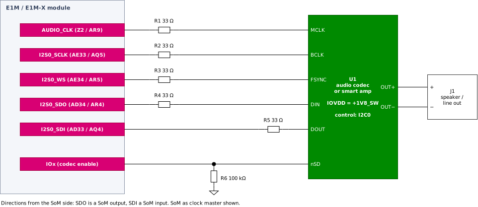
I2S codec or smart amplifier on I2S0, with AUDIO_CLK as MCLK, source series resistors and an enable line with a pull-down
| ID | Strength | Rule | Source |
|---|---|---|---|
| CB-SER-20 | MUST | Supply the I/O of a codec or amplifier from a VIO_OUT-switched rail, so that its outputs (DOUT, and BCLK / FSYNC in clock-master mode) cannot drive the SoM while VIO_OUT is low. | E1M-STD §6.1.2 (3), §6.2.3 (1) |
| CB-SER-21 | SHOULD | Use AUDIO_CLK as the codec MCLK, routed point to point with a series resistor at the pad, and keep all audio clocks away from switching regulators and their planes. | HG-AEN-001 Interfaces; HG-V2N-001 Interfaces |
| CB-SER-22 | SHOULD | Pull the codec shutdown or enable input low (100 kΩ on the E1M EVK) so the codec stays off until firmware enables it, and keep it disabled until the codec I/O rail has settled. | UG-E1M-001 Audio |
| CB-SER-23 | SHOULD | Put the codec control port on a carrier I2C bus at an address clear of the reserved addresses (CB-SER-08, CB-SER-10). | Guide (informative) |
19.6 PDM microphones
Each PDM interface has one clock and one data line, and carries two microphones: one with L/R (SELECT) high and one with L/R low. The two microphones drive the shared data line on opposite clock edges. Two interfaces give up to four microphones.
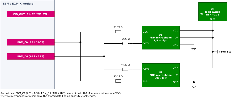
Two PDM microphones on PDM0: shared clock and data with 22 Ω series resistors, opposite L/R straps, supply from a load switch enabled by VIO_OUT
| ID | Strength | Rule | Source |
|---|---|---|---|
| CB-SER-24 | MUST | Supply the microphones from a carrier rail switched by VIO_OUT: not from VIO_OUT itself (not a permitted use) and not from an always-on rail (the data outputs would drive an unpowered SoM). | E1M-STD §6.1.2 (3), §6.2.3 (1) |
| CB-SER-25 | SHOULD | Connect at most two microphones per PDM_Dx line, with opposite L/R straps, and choose microphones whose supply range includes 1.71 V. | DS-AEN-001 PDM; DS-V2N-001 PDM; E1M-STD §6.1.2 (1) |
| CB-SER-26 | SHOULD | Fit a series resistor (22 Ω on the E1M EVK) on the clock and on the data line of each microphone, route PDM_Cx short and away from switching nodes, and decouple each microphone supply pin as its datasheet requires (typically 100 nF). | UG-E1M-001 Audio (series resistors); HG-AEN-001 Interfaces; Guide (informative) (decoupling) |
19.7 Per-module differences
| Item | E1M-AEN | E1M-X V2N | E1M-X V2N-M1 |
|---|---|---|---|
| I2C buses on pads | I2C0, I2C1 | I2C0 to I2C3; I2C3 (A24 / A23) is wired to the GD32G553 I/O MCU and reached through the Alp SDK | As V2N |
I2C0 on-module device | N24S128C4DYT3G at 0x50 / 0x58, powered from the module 1.8 V rail, no write protect | N24S128C4DYT3G at 0x50 / 0x58 (optional per HG-V2N-001) | As V2N |
| On-module pull-ups | None on I2C0 | Not stated | Not stated |
| Other on-module I2C devices | On the private RSVD bus U3 / V3 only; never connect | Board-bus devices in the address table; exposure on pads not confirmed | As V2N, plus the DX-M1 rail regulators; PMIC writes can damage the DX-M1 |
| I2C / I3C pull-up value | 4.7 kΩ (2.2 kΩ if the capacitance requires) | TBD | TBD |
SPI1 | Wi-Fi module SPI (CC3501E), switched with the radio; not usable by the host | SoC SPI | SoC SPI |
SPI2 | No pads (E1M) | SoC SPI | SoC SPI |
AUDIO_CLK | Z2 | AR9 | AR9 |
| PDM | Two interfaces, 1.8 V | Two interfaces, up to four microphones | As V2N |
19.8 Chapter checklist
| ID | Check | Done |
|---|---|---|
| CB-SER-01, 02, 03 | I2C / I3C pull-ups fitted, to VIO_OUT or a VIO_OUT-switched rail only; values checked against bus capacitance and rise time. | ☐ |
| CB-SER-04, 05, 06, 28 | Bus devices on a VIO_OUT-switched rail, or behind a translator whose datasheet guarantees high-impedance ports with the VIO_OUT side off; translator EN not tied to VIO_OUT unless its threshold refers to it. | ☐ |
| CB-SER-08, 09, 10, 29 | No carrier device at 0x50 / 0x58; no second controller on E1M-X buses, none at all on I2C3; E1M-X on-module addresses (both 0x40 and 0x48) kept clear. | ☐ |
| CB-SER-11, 12 | UART adapters referenced to VIO_OUT and high-impedance while it is low; no flow control without a declared dependency. | ☐ |
| CB-SER-14, 15, 17 | E1M SPI1 not driven or pulled up; carrier SPI devices on SPI0; no MISO drive into an unpowered SoM. | ☐ |
| CB-SER-20, 22 | Codec I/O on a VIO_OUT-switched rail; codec enable pulled low. | ☐ |
| CB-SER-24, 25 | Microphones on a VIO_OUT-switched rail; two per data line with opposite L/R straps. | ☐ |
| Pad IDs | No net carried between E1M and E1M-X footprints by pad ID. | ☐ |
20 ADC, DAC, PWM, Encoder and GPIO
The analog, PWM, encoder and GPIO pads are all in the VIO_OUT (1.8 V) domain (E1M-STD §6.7.1). The analog pads therefore follow the same back-powering rules as the digital ones: no voltage source, pull-up or sensor output may push current into them while VIO_OUT is low (E1M-STD §6.2.3 (1)). Which device drives a pad differs between modules; the GPIO owner map in this chapter shows it.
20.1 Pads
| Pad | E1M | E1M-X | Pad | E1M | E1M-X | Pad | E1M | E1M-X |
|---|---|---|---|---|---|---|---|---|
ANA_S0 | A15 | A17 | PWM0 | A6 | A7 | ENC0_X | A10 | A12 |
ANA_S1 | B15 | B17 | PWM1 | B6 | B7 | ENC0_Y | B10 | B12 |
ANA_S2 | A14 | A16 | PWM2 | A5 | A6 | ENC1_X | A9 | A11 |
ANA_S3 | B14 | B16 | PWM3 | B5 | B6 | ENC1_Y | B9 | B11 |
ANA_S4 | A13 | A15 | PWM4 | A4 | A5 | ENC2_X | A8 | A10 |
ANA_S5 | B13 | B15 | PWM5 | B4 | B5 | ENC2_Y | B8 | B10 |
ANA_S6 | A12 | A14 | PWM6 | A3 | A4 | ENC3_X | A7 | A9 |
ANA_S7 | B12 | B14 | PWM7 | B3 | B4 | ENC3_Y | B7 | B9 |
DAC0 | A16 | A19 | ||||||
DAC1 | B16 | B19 |
A GPIO net carried by pad ID from E1M-X IO3 to pad O2 lands on E1M MODULE_STBY and puts an E1M-AEN into standby when driven low, so never carry a net assignment from one footprint to the other by pad ID.
Other collisions of this chapter's pads: E1M A15 is ANA_S0 but E1M-X A15 is ANA_S4; E1M-X A19 is DAC0 while E1M A19 is CAN_STBY; E1M-X IO1 / IO2 (M2 / N2) are E1M SPI0_MOSI / SPI0_SCLK; E1M-X IO5 (AG2) is E1M IO3; E1M IO25 (P3) is E1M-X LCD_B12.
20.2 ADC inputs
The ADC full scale follows the module's 1.8 V rail: E1M-AEN hw_rev R3 has no separate precision reference, and the E1M-X modules state that their analog inputs are referenced to 1V8. VIO_OUT is 1.8 V ± 5 % (E1M-STD §6.1.2 (1)), so a carrier that designs its full-scale signal to 1.71 V stays inside the range on every module. The input impedance of the ADC and the largest source impedance it accepts are not published for any of the three modules.
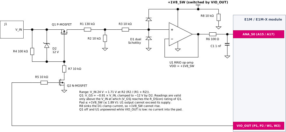
ADC front end for a signal that exists while the SoM is off (here up to 24 V): high-side switch Q1 / Q2 enabled by VIO_OUT with Zener-clamped gate drive D2, divider R1 / R2, current limit R3, clamp D1, follower U1 supplied from the VIO_OUT-switched rail +1V8_SW, bleed load R8, and R6 / C1 at the pad
The divider maps 24 V to 24 V ⋅ 10 kΩ / (130 kΩ + 10 kΩ) = 1.71 V. The pad is not driven by the divider but by the follower U1. Its output cannot rise above its own supply, +1V8_SW, which is at most 1.89 V, so the pad stays below the 1.98 V absolute maximum even when V_IN is over-range. A Schottky clamp to the 1.8 V rail cannot do this on its own: one Schottky drop above a 1.89 V rail is about 2.1 V. D1 only protects the U1 input, and R3 limits its current. At V_IN = 40 V, for example, about 40 μA flows into +1V8_SW through D1. R8 (10 kΩ, at least 171 μA) loads the rail by more than that, so the clamp current cannot raise +1V8_SW or the pull-ups on it. U1 also drives the sampling capacitor of the ADC from a low impedance, so the 9.3 kΩ of R1 ∥ R2 no longer limits the sample rate.
Q1 is switched by Q2, which must switch fully at 1.71 V on its gate. R4 and R7 set VGS(Q1) = −VIN ⋅ R4 / (R4 + R7) ≈ −0.91 ⋅ VIN, and D2 (12 V) clamps it above about 13 V. Below the input voltage at which |VGS| reaches the value at which the datasheet specifies RDS(on), Q1 is off or only partly on, and the body diode blocks, so the reading is low or zero. For a part specified at |VGS| = 2.5 V the valid range starts at about 2.75 V. If the reading must cover 0 V, use a sensor or source supplied from a VIO_OUT-switched rail instead of the high-side switch. The highest input the circuit takes is set by the VDS rating of Q1 and by the dissipation in R7 and D2 (at 40 V: 2.8 mA, 78 mW in R7). A sensor with a 0–1.8 V output, supplied from a VIO_OUT-switched rail, needs no divider and no switch: keep R3, D1, U1, R6 and C1.
| ID | Strength | Rule | Source |
|---|---|---|---|
| CB-ANA-01 | MUST | Keep every ANA_Sx pad between − 0.3 V and 1.98 V at all times, over-range and fault inputs included, and inside 0–1.8 V for valid conversions. | E1M-STD §6.2.3 (5); DS-AEN-001 Abs. Max.; DS-V2N-001 Abs. Max. |
| CB-ANA-02 | MUST | Source no current into an ANA_Sx pad while VIO_OUT is low: switch off any signal that exists while the SoM is off (high-side switch enabled by VIO_OUT, or a sensor supplied from a VIO_OUT-switched rail). | E1M-STD §6.2.3 (1) |
| CB-ANA-03 | MUST NOT | Clamp an analog input to VIO_OUT: clamp current would raise VIO_OUT. Clamp to a carrier rail switched by VIO_OUT and to GND. | E1M-STD §6.1.2 (2), §6.2.3 (4) |
| CB-ANA-04 | MUST | Bound the pad voltage at or below 1.98 V for every input the product can see: drive the pad from a buffer supplied from a VIO_OUT-switched 1.8 V rail (figure), or use a clamp whose datasheet clamping voltage at the worst-case fault current is at or below 1.98 V. A Schottky clamp to the 1.8 V rail alone does not meet CB-ANA-01. | E1M-STD §6.2.3 (5); Guide (informative) |
| CB-ANA-12 | MUST | Give every rail that a clamp feeds a permanent load (or a shunt) that sinks more than the worst-case clamp current, so that clamp current cannot raise the rail or the pads pulled up to it (R8 in the figure). | E1M-STD §6.2.3 (5); Guide (informative) |
| CB-ANA-13 | SHOULD | Choose a rail-to-rail input and output op-amp rated for a 1.71 V supply, with its input current held within the datasheet limit by the series resistor; expect the output to lose the last few millivolts near 0 V. | E1M-STD §6.1.2 (1); Guide (informative) |
| CB-ANA-14 | SHOULD | State the minimum input voltage of a high-side-switched input: the switch is fully on only once its |VGS| reaches the RDS(on) rating. Clamp the gate-source voltage with a Zener when the input can exceed the MOSFET's VGS rating. | Guide (informative) |
| CB-ANA-05 | SHOULD | Fit a series resistor and a capacitor to GND at the pad (100 Ω and 1 nF in the figure) as charge reservoir and anti-alias filter, check the driver's stability with that load, and check the conversion error at the target sample rate, because the ADC input impedance is not published. | Guide (informative) |
| CB-ANA-06 | SHOULD | Where absolute accuracy matters, measure ratiometrically or put a carrier reference on a spare ANA_Sx channel and calibrate against it. | DS-AEN-001 ADC; Guide (informative) |
| CB-ANA-07 | SHOULD | Route analog inputs short, over a continuous ground plane and away from digital and switching nodes. | HG-V2N-001 Interfaces |
20.3 DAC outputs
DAC0 and DAC1 are 12-bit outputs referenced to the module 1.8 V rail, with a 1 kHz update rate on all three modules. Their output drive is not published, so the carrier buffers them.
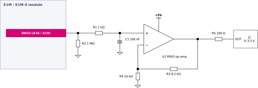
DAC buffer: pull-down R2 defines 0 V while the SoM is off, R1 / C1 smooth the 1 kHz steps, and op-amp U1 scales 0–1.8 V to 0–3.3 V (gain 1 + R3 / R4 = 1.82)
| ID | Strength | Rule | Source |
|---|---|---|---|
| CB-ANA-08 | SHOULD | Buffer each DAC pad with a high-impedance (CMOS-input) op-amp before any cable, connector or load. | DS-AEN-001 DAC; DS-V2N-001 DAC; Guide (informative) |
| CB-ANA-09 | MUST | Source no current into a DAC pad while VIO_OUT is low: no pull-up, and a buffer input whose bias and protection paths do not feed the pad. | E1M-STD §6.2.3 (1) |
| CB-ANA-10 | SHOULD | Fit a high-value pull-down (1 MΩ in the figure) at the buffer input, so that the buffered output is defined while the SoM is off or booting. | E1M-STD §6.2.3 (1); Guide (informative) |
| CB-ANA-11 | SHOULD | Add a reconstruction filter matched to the 1 kHz update rate (1 kΩ and 100 nF give about 1.6 kHz). | Guide (informative) |
20.4 PWM and quadrature encoders
PWMx are SoM outputs; ENCx_X / ENCx_Y are SoM inputs. Encoders usually run at 5 V or 3.3 V, or have open-collector outputs, so their signals reach the pads through a translator that isolates both sides while VIO_OUT is off.
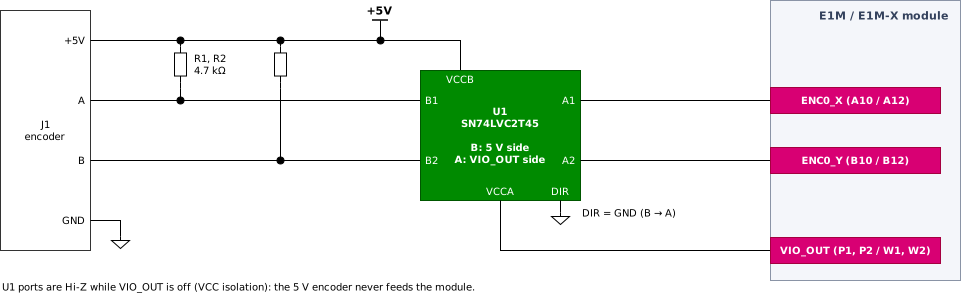
5 V encoder to ENC0_X / ENC0_Y: pull-ups on the encoder side and a dual-supply translator U1 with VCCA from VIO_OUT and DIR tied for B to A
| ID | Strength | Rule | Source |
|---|---|---|---|
| CB-PWM-01 | MUST | Connect encoders that are not on a VIO_OUT-switched 1.8 V rail through a translator referenced to VIO_OUT whose ports are high-impedance while VCCA is off (for example SN74LVC2T45, VCC isolation). | E1M-STD §6.1.2 (5), §6.2.3 (1), (5) |
| CB-PWM-02 | SHOULD | Put open-collector pull-ups on the encoder side of the translator, never on the pads; receive differential (RS-422) encoders with a line receiver ahead of the translator. | Guide (informative) |
| CB-PWM-03 | SHOULD | Choose translators whose VCCA range covers 1.65–3.6 V. | E1M-STD §6.1.2 (informative note) |
| CB-PWM-04 | SHOULD | Hold every PWM-driven load off while the SoM is off or booting: a pull-down (for example 100 kΩ) at the driver or MOSFET-gate input. | E1M-STD §6.2.3 (1); Guide (informative) |
| CB-PWM-05 | SHOULD | Drive 3.3 V or 5 V loads through a translator referenced to VIO_OUT, or a logic-level MOSFET whose gate threshold is fully met at 1.71 V. | E1M-STD §6.1.2 (1); Guide (informative) |
20.5 GPIO
20.5.1 Owners per module
On every module the default GPIO pads IO0 to IO35 are driven by different devices: the SoC, an on-module radio, the I/O MCU or the DX-M1. The owner decides the pad's timing (an I/O-MCU pad is reached through the module's bridge firmware), its power island (radio pads are off while the radio is off) and whether the carrier may drive it at all.
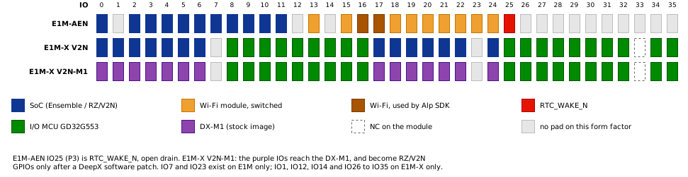
GPIO owner map, IO0 to IO35, for each reference module
| Pad | E1M | E1M-X | Pad | E1M | E1M-X | Pad | E1M | E1M-X |
|---|---|---|---|---|---|---|---|---|
IO0 | L2 | L2 | IO12 | — | AR23 | IO24 | O3 | AR29 |
IO1 | — | M2 | IO13 | E3 | AQ23 | IO25 | P3 | F63 |
IO2 | W2 | N2 | IO14 | — | AR24 | IO26 | — | F64 |
IO3 | AG2 | O2 | IO15 | F3 | AQ24 | IO27 | — | AN63 |
IO4 | AG16 | AF2 | IO16 | G3 | AR25 | IO28 | — | AN64 |
IO5 | AH18 | AG2 | IO17 | H3 | AQ26 | IO29 | — | AO63 |
IO6 | AG18 | AL2 | IO18 | I3 | AR26 | IO30 | — | AO64 |
IO7 | AG34 | — | IO19 | J3 | AQ27 | IO31 | — | AP63 |
IO8 | AG33 | AR21 | IO20 | K3 | AR27 | IO32 | — | AP64 |
IO9 | AH34 | AQ21 | IO21 | L3 | AQ28 | IO33 | — | AQ63 |
IO10 | AH33 | AR22 | IO22 | M3 | AR28 | IO34 | — | AQ64 |
IO11 | A18 | AQ22 | IO23 | N3 | — | IO35 | — | A25 |
On E1M, IO0 and IO2 to IO11 are SoC GPIOs on E1M-AEN, the only E1M module so far. On E1M-X, only the I/O-MCU pads IO8 to IO16, IO25 to IO32, IO34 and IO35 behave the same on V2N and V2N-M1; IO0 to IO6, IO17 to IO22 and IO24 reach the DX-M1 on V2N-M1 with the stock image. Put carrier enables, resets and interrupts on the safe pads first.
20.5.2 GPIO rules
| ID | Strength | Rule | Source |
|---|---|---|---|
| CB-GPIO-01 | MUST | Drive GPIO pads only while VIO_OUT and PORn are high, and pull them up only to VIO_OUT or a VIO_OUT-switched rail. | E1M-STD §6.2.3 (1), (3), (4); HG-AEN-001 Interfaces |
| CB-GPIO-02 | MUST | On E1M, never drive or pull up the E1M-AEN Wi-Fi GPIO pads IO13, IO15 to IO24 (E3, F3, G3, H3, I3, J3, K3, L3, M3, N3, O3) while the radio is off, also while VIO_OUT is high; pull-downs are allowed. | E1M-STD §6.2.3 (7); DS-AEN-001 Pin Description |
| CB-GPIO-03 | MUST | On E1M-X, keep IO0 to IO6, IO17 to IO22 and IO24 (L2, M2, N2, O2, AF2, AG2, AL2, AQ26, AR26, AQ27, AR27, AQ28, AR28, AR29) high-impedance or input-only in every build variant that supports V2N-M1: they reach the on-module DX-M1, and a carrier output would contend with it. | DS-V2N-M1-001 Pin Description |
| CB-GPIO-04 | MUST NOT | Use a pad of the set GND, NC, RSVD, POWER_*, ANT_*, BL_LED_A, BL_LED_K as GPIO. | E1M-STD §8.2 |
| CB-GPIO-05 | MUST | When the carrier uses a non-GPIO pad as GPIO, stay hardware-compatible with a SoM that routes only the default function: treat the pad as default-driven (for example never drive a pad whose default function is an output) until GPIO software is loaded. | E1M-STD §8.2 |
| CB-GPIO-06 | MUST | Use a tertiary function only with a per-SoM dependency declared in the carrier build system, rejecting SoMs whose manifest does not expose it. | E1M-STD §8.4 |
| CB-GPIO-07 | MUST NOT | Fit a pull-up from E1M IO25 (P3) to an always-on or 3.3 V rail in the default fit: on any E1M module other than E1M-AEN, IO25 is a 1.8 V GPIO with a 1.98 V absolute maximum. | E1M-STD §6.2.3 (4), (5) |
| CB-GPIO-08 | MAY | For E1M-AEN RTC_WAKE_N on IO25 (open drain, active low, valid while VDD_5V_IN is present), use one of two pull-ups. Any module, default fit: a pull-up to a VIO_OUT-switched rail (E1M EVK 2641-R3: R256 100 kΩ to +VIO_SW); it reports no wake while the module is off. E1M-AEN only: the pull-up DS-AEN-001 recommends, ≥ 10 kΩ to the host's always-on rail (≤ 5.5 V), as a not-fitted-by-default option in a build variant declared for E1M-AEN. That option relies on the SoM declaring IO25 outside the VIO_OUT domain. | E1M-STD §6.7.1, §6.2.3 (2), (4); DS-AEN-001 Pin Description; UG-E1M-001 Module Control Pins |
| CB-GPIO-09 | SHOULD NOT | Use E1M-AEN IO16 and IO17: the current Alp SDK Wi-Fi firmware reserves them. | DS-AEN-001 Pin Description |
| CB-GPIO-10 | SHOULD | Define every carrier input that a GPIO controls (enables, resets, mux selects) with its own pull-down, or a pull-up to a VIO_OUT-switched rail, at the load: pad reset states are not published. | E1M-STD §6.6; UG-E1M-001 Jumpers |
| CB-GPIO-11 | SHOULD | Give GPIO lines that leave the board a series resistor and ESD protection (Chapter 22). | Guide (informative) |
20.6 Per-module differences
| Item | E1M-AEN | E1M-X V2N | E1M-X V2N-M1 |
|---|---|---|---|
| ADC | SoC, 8 channels, 12-bit, up to 5 Msps | I/O MCU GD32G553, 8 channels, 12-bit, 5.3 Msps | As V2N |
| ADC range, absolute maximum | 0–1.8 V; − 0.3 V to 1.98 V | 0–1.8 V; − 0.3 V to 1.98 V | As V2N |
| ADC reference | Module 1.8 V rail; no precision reference on hw_rev R3 | Referenced to 1V8 | As V2N |
| ADC input impedance, source limit | Not published | TBD | TBD |
| DAC | SoC, 2 channels, 12-bit, 1 kHz; drive not published | I/O MCU, 2 channels, 12-bit, 1 kHz; drive TBD | As V2N |
| PWM | SoC, 8 outputs | I/O MCU, 8 outputs | As V2N |
| GPIO owners | SoC: IO0, IO2 to IO11 (IO8 to IO10 can wake the SoC from STOP). Wi-Fi module CC3501E: IO13, IO15 to IO24, switched with the radio; IO16, IO17 used by the Alp SDK. | RZ/V2N: IO0 to IO6, IO17 to IO22, IO24. I/O MCU: IO8 to IO16, IO25 to IO32, IO34, IO35. | As V2N, but IO0 to IO6, IO17 to IO22, IO24 reach the DX-M1; RZ/V2N GPIO only after a DeepX software patch. |
IO25 | P3, RTC_WAKE_N, open drain, 5 V tolerant | F63, I/O-MCU GPIO | As V2N |
IO33 | No pad (E1M) | AQ63, not connected on the module | As V2N |
20.7 Chapter checklist
| ID | Check | Done |
|---|---|---|
| CB-ANA-01, 02 | Every ANA_Sx input stays within − 0.3 V to 1.98 V and carries no current while VIO_OUT is low. | ☐ |
| CB-ANA-03, 04, 12 | No clamp to VIO_OUT; pad bounded at or below 1.98 V for every input (buffer on a VIO_OUT-switched rail, not a Schottky clamp alone); clamp rail loaded beyond the worst-case clamp current. | ☐ |
| CB-ANA-13, 14 | Op-amp rated for a 1.71 V supply; minimum valid input of a switched input stated. | ☐ |
| CB-ANA-05 | Pad capacitor fitted and conversion error checked at the target sample rate. | ☐ |
| CB-ANA-08, 09, 10 | DAC outputs buffered by a CMOS-input op-amp, with a pull-down and no pull-up. | ☐ |
| CB-PWM-01, 02 | Encoders reach the pads through a translator that is high-impedance with VCCA off; pull-ups on the encoder side. | ☐ |
| CB-PWM-04 | Every PWM-driven load is held off by a pull-down while the SoM is off or booting. | ☐ |
| CB-GPIO-01, 02, 03 | No GPIO drive before VIO_OUT and PORn are high; E1M-AEN Wi-Fi pads and V2N-M1 DX-M1 pads not driven. | ☐ |
| CB-GPIO-04, 05, 06 | No GPIO use of excluded pads; default-function compatibility kept; tertiary functions declared. | ☐ |
| CB-GPIO-07, 08 | No always-on pull-up on E1M IO25 in the default fit; any RTC_WAKE_N pull-up goes to a VIO_OUT-switched rail, or to the always-on rail only as an E1M-AEN-only option. | ☐ |
| CB-GPIO-10 | Every GPIO-controlled carrier input has its own defined default. | ☐ |
21 Thermal Design
An E1M or E1M-X module has no thermal pad of its own. Its heat leaves mainly through the LGA pads, above all the GND pads, into the carrier copper, and from the carrier surfaces into the air. The carrier therefore sets most of the module's thermal performance. The module datasheets give SoC package figures (E1M-AEN) or leave the thermal figures TBD (E1M-X), and state that carrier copper area, via stitching and airflow change the result.
All module-level thermal figures available today are estimates or TBD. No module datasheet publishes a measured module-to-ambient thermal resistance. Validate the module temperature in your own enclosure, at your hottest workload, before you freeze the carrier layout.
21.1 Heat path: SoC to module PCB to carrier
The heat sources sit on the top side of the module: the SoC on every module, and on E1M-X V2N-M1 also the DeepX DX-M1 accelerator. The heat flows:
- from the SoC (and the DX-M1) into the module PCB;
- through the soldered LGA pads, mainly the
GNDpads (49 on E1M, 105 on E1M-X), into the carrier top copper; - through vias into the inner ground planes, which spread it across the carrier;
- from both carrier surfaces into the air by convection, and from the module top into the air or into a heatsink.
Steps 2 and 3 are the ones the carrier designer controls. A carrier without inner planes, with few GND vias or with a small copper area loses most of the spreading.
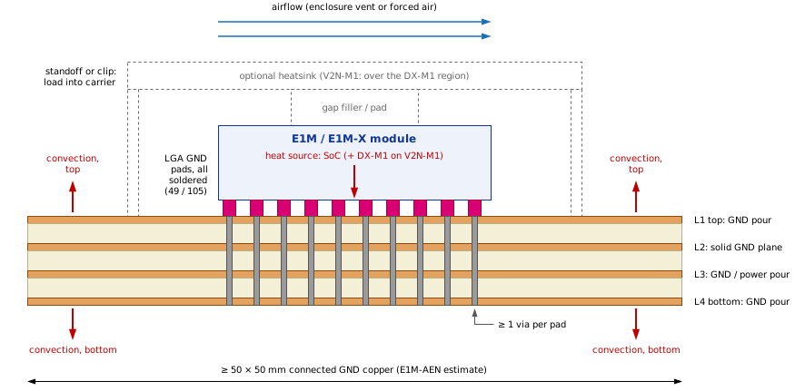
Heat path from the module through the LGA GND pads and vias into the carrier planes, with the optional heatsink and its load path (dashed: not fitted by default)
21.2 Carrier copper and via arrays
| ID | Strength | Rule | Source |
|---|---|---|---|
| CB-THM-01 | MUST | Solder every GND pad of the module and connect each one to a low-impedance ground plane. Do not leave a GND pad open to gain routing space. | E1M-STD §7.3.1, §9.2 (3) |
| CB-THM-02 | SHOULD | Give every GND pad at least one via to a solid ground plane. Place the via next to the pad (or in the pad, filled and capped, where the fabricator supports it), not at the end of a long trace. | DS-AEN-001 Thermal Characteristics; HG-AEN-001 Thermal Design |
| CB-THM-03 | SHOULD | Use at least 4 layers and provide at least 50 × 50 mm of connected GND copper around the module. With this, E1M-AEN reaches a module-to-ambient thermal resistance of about 15 °C/W (estimated). Treat the same area as the minimum for E1M-X; no E1M-X figure is published. | DS-AEN-001 Thermal Characteristics (estimate); Guide (informative) for E1M-X |
| CB-THM-04 | SHOULD | Pour ground copper on the inner and bottom layers under and around the module, and stitch the pours together with a dense via array around the pad ring. Avoid plane splits and long slots under the module: they cut the heat-spreading path as well as the signal return path. | HG-AEN-001 Thermal Design; DS-V2N-001 Thermal Characteristics |
| CB-THM-05 | SHOULD | Keep carrier heat sources (5 V buck converter, eFuse, linear regulators, backlight LEDs, M.2 devices) out of the copper area that spreads the module's heat, or place them downstream in the airflow. | Guide (informative) |
The carrier copper under the module also carries the return currents of every high-speed interface. The thermal rules above and the ground rules of Chapter 4 point the same way; there is no trade-off between them.
21.3 Enclosure, airflow, derating and heatsinks
| ID | Strength | Rule | Source |
|---|---|---|---|
| CB-THM-06 | SHOULD | Validate the module temperature in the target enclosure early, at the hottest workload: sustained NPU inference with Wi-Fi transmitting (E1M-AEN); DRP-AI3 and DX-M1 running together (E1M-X V2N-M1). Plan enclosure ventilation from the start; even modest forced airflow lowers the module temperature significantly. | HG-AEN-001 Thermal Design; DS-V2N-M1-001 Thermal Characteristics |
| CB-THM-07 | SHOULD | For a carrier that hosts any module, specify the product ambient within −40 °C to +75 °C, the range that every current module supports. Rate carrier parts for the product ambient plus their own temperature rise. A carrier that declares (E1M-STD §9.2 (2)) that it hosts only E1M-X V2N or V2N-M1 modules may use −40 °C to +85 °C. | DS-AEN-001 Recommended Operating Conditions; DS-V2N-001, DS-V2N-M1-001 Environmental Conditions |
| CB-THM-08 | SHOULD | Choose the RTC backup store on +S_CAP (Chapter 10) for the product temperature range: the store, not the module, sets the range over which the RTC keeps time without 5 V. | DS-AEN-001 Recommended Operating Conditions (note) |
| CB-THM-09 | SHOULD | Plan application derating for a high ambient: cap the Wi-Fi transmit power and duty, and the AI workload or clock. E1M-AEN planning values on a 50 × 50 mm carrier in natural convection: Wi-Fi TX at ≤ 30 % duty, TA ≤ 60 °C; continuous 18 dBm TX, TA ≤ 40 °C or forced air ≥ 1 m/s (estimated). | HG-AEN-001 Thermal Design |
| CB-THM-10 | SHOULD | Limit the backlight LED power driven from the on-module driver to ≤ 0.8 W (Chapter 16). | HG-AEN-001 Thermal Design; DS-AEN-001 Thermal Characteristics |
| CB-THM-11 | MUST | Carry the clamping force of any heatsink, gap filler or enclosure contact on the module into the carrier through standoffs, clips or the enclosure. The LGA solder joints must not carry the heatsink mass or a static clamping force, because that cracks the joints over temperature cycles. | Guide (damage: cracked LGA joints); see also HG-V2N-M1-001 Handling and Assembly ("avoid mechanical stress after soldering") |
| CB-THM-12 | SHOULD | On E1M-X V2N-M1, provide copper-pour or heatsink contact over the DX-M1 region of the module, and active cooling or forced air above about 50 % DX-M1 utilisation. Use a soft gap filler, so that the clamping force stays low (CB-THM-11). | DS-V2N-M1-001 Thermal Characteristics; HG-V2N-M1-001 Design Checklist |
| CB-THM-13 | SHOULD | Check the vertical clearance for a heatsink against the module height above the carrier: the module height, plus the spacer thickness with mounting option (a) (Chapter 3, CB-MEC-09). The module height and the spacer thickness are still TBD in the specification (E1M-STD §5.2; Annex C, C-34): leave margin and confirm the height with Alp Lab before you fix a heatsink drawing. | E1M-STD §5.2; HG-V2N-M1-001 Dimensions; Alp Lab, 2026-10-19 |
A heatsink that is screwed or pressed onto the module without its own load path to the carrier cracks the LGA solder joints.
The θJA and θJC values in the E1M-AEN datasheet (21.1 °C/W still air, 17.0 °C/W) are the SoC package values, not the module-on-carrier value. As a rule of thumb with the E1M-AEN estimate of about 15 °C/W module-to-ambient, each watt of module dissipation raises the module about 15 °C above the ambient.
21.4 Per-module figures
| Parameter | E1M-AEN | E1M-X V2N | E1M-X V2N-M1 |
|---|---|---|---|
| Ambient operating temperature | −40 to +75 °C (Ensemble SoC limit); room-temperature assembly option with on-module supercap −20 to +60 °C | −40 to +85 °C | −40 to +85 °C |
| Storage temperature | −40 to +125 °C | −40 to +125 °C | −40 to +125 °C |
| Maximum junction temperature | +105 °C operating, +150 °C absolute | TBD | TBD (RZ/V2N and DX-M1) |
| Thermal resistance | θJA 21.1 °C/W, θJC 17.0 °C/W (SoC package); about 15 °C/W module-to-ambient on ≥ 50 × 50 mm GND copper (estimated) | θJA, θJB TBD | θJA,V2N, θJA,M1 TBD |
| Power-dissipation derating | 67 mW/°C on a 50 × 50 mm carrier (estimated) | TBD (above +85 °C) | TBD (above +85 °C) |
GND pads | 49 | 105 | 105 |
| Heat sources | SoC; hottest case NPU inference with Wi-Fi TX | SoC | SoC and DX-M1, concurrent under AI load |
| Cooling recommendation | copper area and via stitching; forced air ≥ 1 m/s for continuous 18 dBm TX above 40 °C (estimated) | carrier copper, airflow, via stitching | active heatsink or forced air above about 50 % DX-M1 utilisation |
| Height class in the module documents (replaced by the mounting options, Chapter 3) | not stated | not stated | standard (DX-M1, LPDDR5X and SPI NAND on the top side) |
21.5 Chapter checklist
| ID | Check | Done |
|---|---|---|
| CB-THM-01 | Every GND pad soldered and connected to a ground plane. | ☐ |
| CB-THM-02 | At least one via per GND pad, next to the pad. | ☐ |
| CB-THM-03 | ≥ 4 layers; ≥ 50 × 50 mm connected GND copper around the module. | ☐ |
| CB-THM-04 | Inner and bottom pours stitched; no plane split under the module. | ☐ |
| CB-THM-05 | Carrier heat sources kept out of the module's spreading area. | ☐ |
| CB-THM-06 | Module temperature validated in the enclosure at the hottest workload. | ☐ |
| CB-THM-07 | Product ambient within −40 to +75 °C (any module), or the hosted SoM set declared. | ☐ |
| CB-THM-08 | RTC backup store rated for the product temperature range. | ☐ |
| CB-THM-09 | Application derating for Wi-Fi TX and AI load defined. | ☐ |
| CB-THM-10 | Backlight LED power ≤ 0.8 W (E1M-AEN). | ☐ |
| CB-THM-11 | Heatsink or enclosure force carried by standoffs, not by the LGA joints. | ☐ |
| CB-THM-12 | V2N-M1: copper or heatsink contact over the DX-M1 region; cooling plan above 50 % DX-M1 load. | ☐ |
| CB-THM-13 | Heatsink clearance checked against the module height plus, with a spacer PCB, the spacer thickness. | ☐ |
22 EMC and ESD Protection
The ESD ratings of a module apply at its LGA pads during assembly (HBM and CDM component ratings). They are not system-level ratings. A pad that reaches a connector, a header, a button or any other point a user or a cable can touch needs protection on the carrier. E1M-STD §10.4 also states that conformance to the specification does not replace the EMC and safety approvals of the end product.
22.1 Principle
| ID | Strength | Rule | Source |
|---|---|---|---|
| CB-EMC-01 | MUST | Protect every carrier connector, header, button and test access that leads to a module pad, unless every SoM in the carrier's declared SoM set (E1M-STD §9.2 (2)) declares on-module protection for that interface. For a carrier that hosts any module, assume no on-module protection on any interface: the specification does not require it, and a future conformant module may have none. | Guide (damage); DS-AEN-001, DS-V2N-001, DS-V2N-M1-001 ESD & Latch-up Ratings; HG-V2N-001 rev 0.2 |
| CB-EMC-02 | MUST | Choose each protection part for the voltage domain of the pad it protects (E1M-STD §6.7.1): its working voltage must cover the highest level the pad can carry, and it must not clamp a pad below that level. Examples: ≥ 5.5 V on MODULE_EN; the SD_VDD level on the SD lines (3.4 V on E1M-AEN); up to 36 V on BL_LED_A (E1M-AEN); bus level on bus-level CAN pads. | E1M-STD §6.3.1 (1), §6.7.1; DS-AEN-001 Absolute Maximum Ratings |
| CB-EMC-03 | MUST | Do not connect the supply pin of a rail-referenced (steering-diode) ESD array to VIO_OUT, SD_VDD / SD_VDD_OUT, +V_CAMx or any other module output rail. A signal from outside then feeds that rail through the array while the module is off. Use GND-referenced arrays on module lines, or reference the array to a carrier rail. | E1M-STD §6.1.2 (2), §6.2.3 (1), §6.7.1 |
The module datasheets give the pad ratings as component ratings: E1M-AEN HBM ± 2000 V (JS-001), CDM ± 250 V (JS-002), latch-up ± 50 mA (JESD78). The E1M-X V2N and V2N-M1 ratings are TBD. Pick the system-level ESD level (for example the IEC 61000-4-2 level) from the standard that applies to your end product.
22.2 Per-interface protection
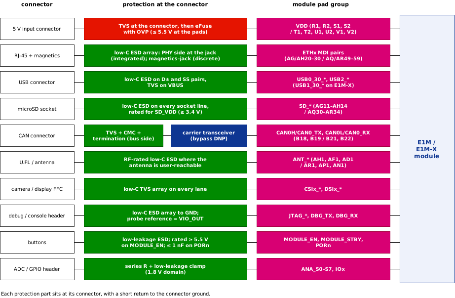
Protection placement: each connector, its protection part class at the connector, and the module pad group it serves. CAN protection sits on the bus side of the carrier transceiver (safe default; bypass not fitted)
| Interface | Pads (E1M / E1M-X) | On the module | Carrier protection | ID |
|---|---|---|---|---|
| 5 V input | VDD (R1, R2, S1, S2) / VDD_5V_IN (T1, T2, U1, U2, V1, V2) | none on any module | TVS at the input connector, ahead of an eFuse or load switch with over-voltage cut-off; a TVS alone does not hold 5.5 V (Chapter 5). | CB-EMC-04 |
| Ethernet MDI | ETH0_* (AG27–AH30) / (AQ56–AR59); ETH1_* (AG20–AH23) / (AQ49–AR52) | E1M-AEN: DP83825 MDI pins ± 5 kV HBM (component rating, not IEC 61000-4-2). V2N / V2N-M1: none | Low-capacitance ESD array on every port brought to a connector. Discrete magnetics: between the magnetics and the jack. Transformer-integrated RJ-45: on the PHY side, at the jack pins. Common-mode choke where needed. 2641-R3 precedent: HR851178A (integrated magnetics) with one TPD4E05U06DQAR per two pairs on the PHY side. | CB-EMC-05 |
| USB | USB0_30_*, USB2_* / USB0_30_*, USB1_30_*, USB2_20_*; USB_CC1, USB_CC2 (A2, B2) | none stated | Low-capacitance ESD on D± and on the SuperSpeed pairs, TVS on the connector VBUS, ESD on CC at a Type-C connector. 2641-R3 precedent: discrete ESD diodes on the host-port D±. | CB-EMC-06 |
| SD card | SD_CLK, SD_CMD, SD_D0–SD_D3, SD_DET, SD_RST | E1M-AEN: NVT4858HKZ on CLK, CMD, DAT (± 8 kV contact, ± 15 kV air); SD_DET, SD_RST unprotected. V2N / V2N-M1: ESD and 22 Ω series resistors on the SDIO lines | Low-capacitance ESD on every socket line: SD_CLK, SD_CMD, SD_D0–SD_D3 rated for the SD_VDD domain (working voltage ≥ 3.4 V); SD_DET (and SD_RST if it reaches the socket), which are VIO_OUT-domain (1.8 V) pads. 2641-R3 precedent: ESD9101P2T5G on every socket line. | CB-EMC-07 |
| MIPI CSI-2, DSI | CSIx_*, DSIx_* | none | Low-capacitance TVS array on every lane at the camera or display connector. HG-AEN-001 precedent: RCLAMP3552T.TNT. | CB-EMC-08 |
| CAN | CAN0H/CAN0_TX (B18 / B21), CAN0L/CAN0_RX (B19 / B22); E1M-X CAN1 (B24, B25) | E1M-AEN PHY option: TCAN1044AVDRBRQ1 (ISO 10605 ± 8 kV contact, ± 15 kV air); standard build: none (logic-level). V2N / V2N-M1: on-module transceivers, rating not stated | TVS and common-mode choke at the connector, with the termination, on the bus side of the carrier transceiver (the default fit; bypass not fitted). Never directly on a module pad that can be logic-level (Chapter 18). 2641-R3 precedent: PESD2IVN24-UX and DLW43SH510XK2L. | CB-EMC-09 |
| Antenna | ANT_2.4GHZ (AH1 / AR1), ANT_5GHZ (AF1 / AP1), ANT_6GHZ (AD1 / AN1) | E1M-AEN radio module: ± 4 kV contact, ± 8 kV air (EN 301-489). V2N / V2N-M1: not stated | Where the antenna or its connector is user-reachable: an RF-rated ESD part whose capacitance does not detune the 50 Ω feed at the highest band used. An internal chip antenna needs none. | CB-EMC-10 |
| Debug and console | JTAG_* (X1, X2, Y1, Y2, Z1 / AJ1, AJ2, AK1, AK2, AL1), DBG_TX, DBG_RX (AD3, AE3 / AC62, AD62) | none | Low-capacitance, GND-referenced ESD array where the header is reachable from outside the enclosure. Its capacitance counts against the PORn limit if PORn is on the header. | CB-EMC-11 |
| Control buttons | MODULE_EN (O1 / AA1), MODULE_STBY (O2 / AB1), PORn (W1 / Z1) | none | Low-leakage ESD diode; no debounce capacitor preferred. Any capacitance on PORn counts against the 1 nF budget (CB-EMC-15). | CB-EMC-12 |
| ADC and GPIO headers | ANA_S0–ANA_S7, IOx | none | Series resistor and low-leakage clamp; inputs stay within 0–1.8 V, absolute maximum 1.98 V. | CB-EMC-13 |
| ID | Strength | Rule | Source |
|---|---|---|---|
| CB-EMC-04 | MUST | Place a TVS at the 5 V input connector, ahead of the over-voltage cut-off that keeps VDD_5V_IN at or below 5.5 V. | Guide (damage) for the TVS; E1M-STD §6.1.1 (2), (6) for the over-voltage protection; HG-AEN-001 Protection |
| CB-EMC-05 | MUST | Provide a low-capacitance ESD array on the MDI lines of every Ethernet port brought to a connector, rated for the MDI of every hosted module (E1M-AEN DP83825, 100BASE-TX; E1M-X RTL8211FI-VD-CG, 1000BASE-T). With discrete magnetics, place it between the magnetics and the connector. With a transformer-integrated RJ-45, which has no accessible point between magnetics and jack, place it on the PHY side, at the jack pins (2641-R3: D35, D39 on J8; D40, D41 on J20). | E1M-STD §7.3.6 (2) (location wording: Annex C, C-31); UG-E1M-001 Ethernet |
| CB-EMC-06 | MUST | Protect every external USB connector: D±, SuperSpeed pairs, VBUS and, on Type-C, CC. | DS-AEN-001 ESD & Latch-up Ratings (carrier protects all external interfaces); Guide |
| CB-EMC-07 | MUST | At a user-accessible card slot, protect every socket line: SD_CLK, SD_CMD, SD_D0–SD_D3 with low-capacitance parts rated for the SD_VDD domain (working voltage ≥ 3.4 V), and SD_DET (SD_RST if routed to the socket). A carrier MAY omit the data-line parts only if every SoM in its declared SoM set declares on-module SD protection (E1M-AEN, V2N and V2N-M1 do today). | Guide (damage); E1M-STD §6.7.1; DS-AEN-001 SD Card; DS-V2N-001 SD Card |
| CB-EMC-08 | MUST | Protect the CSI and DSI lanes at every external camera or display connector with a low-capacitance TVS array. | DS-AEN-001, DS-V2N-001 MIPI sections; HG-V2N-001 rev 0.2 |
| CB-EMC-09 | MUST | Put CAN TVS, choke and termination at the connector, on the bus side of the carrier transceiver; never directly on a CAN pad unless every declared SoM implements that group as bus-level CAN. | E1M-STD §7.3.14, §6.7.2; HG-V2N-001 CAN-Bus |
| CB-EMC-10 | SHOULD | Protect a user-reachable antenna connector with an RF-rated ESD part. | Guide (informative) |
| CB-EMC-11 | SHOULD | Protect a debug or console header that is reachable from outside the enclosure. | Guide (informative) |
| CB-EMC-12 | MUST | Protect user buttons on control pads with low-leakage ESD diodes, within the leakage and capacitance limits below. | Guide (damage: user-touchable pad); limits from E1M-STD §6.3.1; DS-AEN-001 Reference Carrier Configurations |
| CB-EMC-13 | SHOULD | Protect analog and GPIO header inputs with a series resistor and a low-leakage clamp. | Guide (informative); DS-AEN-001 Absolute Maximum Ratings |
22.3 Leakage- and capacitance-critical nodes
On some pads the protection part itself can break the module. Count the protection leakage and capacitance against the limits below, at the worst-case temperature.
| ID | Strength | Rule | Source |
|---|---|---|---|
| CB-EMC-14 | MUST | Keep the total carrier leakage on MODULE_EN (O1 / AA1) and on MODULE_STBY (O2 / AB1), ESD part included, at or below 0.1 μA with the carrier driver released (E1M-AEN only value, applies to every module). On MODULE_EN, specify the ESD part leakage at 5.5 V: a module may pull the pad up to VDD_5V_IN. | E1M-STD §6.3.1 (1), (2) |
| CB-EMC-15 | MUST | Keep the total capacitance that the carrier adds on PORn (W1 / Z1), ESD part, test point and button wiring included, at or below 1 nF (E1M-AEN only value, applies to every module). A debounce capacitor counts against this budget; fit none if possible. The 2641-R3 reset circuit (C1 1 nF at button S1) uses the whole budget, so the same circuit with an ESD diode and a test point exceeds 1 nF (Annex C, C-32). | E1M-STD §6.3.1 (3); DS-AEN-001 Reference Schematic; UG-E1M-001 Reset |
| CB-EMC-16 | SHOULD | Keep the total leakage on +S_CAP (AG15 / AQ25), ESD diode, holder and board included, at or below 10 nA (E1M-AEN value; no other module states one). | DS-AEN-001 Electrical Characteristics |
| CB-EMC-17 | SHOULD | Count the leakage of every always-on TVS and ESD part in the standby current budget of battery-powered carriers. | HG-AEN-001 Battery-powered Carriers |
A leaky ESD diode or a pull-up to a switched rail on MODULE_EN holds the module off or makes it restart at random.
22.4 Layout for ESD return paths and chassis ground
| ID | Strength | Rule | Source |
|---|---|---|---|
| CB-EMC-18 | SHOULD | Place each protection part at its connector, before any other part on the line (on Ethernet: as in CB-EMC-05), with its ground pin on a via to the ground plane right at the part. Keep the ESD current path from the connector to ground short and away from the module footprint. | HG-AEN-001 Power Layout; Guide (informative) |
| CB-EMC-19 | SHOULD | Connect connector shields to the carrier ground or chassis through a defined network rather than leaving them floating. 2641-R3 precedent on the RJ-45 shields: 1 nF in parallel with 1 MΩ to 0 V. | Guide (informative); EVK 2641-R3 |
| CB-EMC-20 | SHOULD | Keep switching converters and their hot loops away from the antenna feed, the MIPI lanes and analog inputs; filter the 5 V input at the connector. | HG-AEN-001 PCB Layout; HG-V2N-001 Wi-Fi and BLE |
| CB-EMC-21 | SHOULD | Route no high-speed pair across a plane split or a gap between ground and chassis; use stitching capacitors where a return path must cross. | Guide (informative); Chapter 4 |
22.5 Per-module differences
| Item | E1M-AEN | E1M-X V2N | E1M-X V2N-M1 |
|---|---|---|---|
| Pad HBM / CDM / latch-up | ± 2000 V / ± 250 V / ± 50 mA | TBD | TBD |
| SD data lines | on-module NVT4858HKZ, ± 8 kV contact / ± 15 kV air; SD_DET, SD_RST unprotected (carrier ESD still required for any module, CB-EMC-07) | on-module ESD + 22 Ω series | as V2N |
| Ethernet MDI | DP83825 MDI pins ± 5 kV HBM (component rating, not IEC 61000-4-2); carrier IEC 61000-4-2 ESD required | none on module | none on module |
| CAN | standard build: logic-level pads, no protection; PHY option: TCAN1044AVDRBRQ1 ± 8 kV / ± 15 kV ISO 10605 | on-module transceivers; rating not stated | as V2N |
| Radio | module rated ± 4 kV contact / ± 8 kV air (EN 301-489) | not stated | not stated |
| MIPI, USB, debug | none on module | none on module | none on module |
MODULE_EN / MODULE_STBY leakage limit | ≤ 0.1 μA; 5 V tolerant | not stated (spec value applies) | not stated (spec value applies) |
+S_CAP leakage limit | ≤ 10 nA | not stated | not stated |
22.6 Chapter checklist
| ID | Check | Done |
|---|---|---|
| CB-EMC-01 | Every external connector, header and button that reaches a module pad is protected. | ☐ |
| CB-EMC-02 | Every protection part rated for the domain of its pad (5.5 V on MODULE_EN, SD_VDD, 36 V on BL_LED_A, bus-level CAN). | ☐ |
| CB-EMC-03 | No steering-diode array referenced to VIO_OUT or another module output rail. | ☐ |
| CB-EMC-04 | TVS at the 5 V connector, ahead of the over-voltage cut-off. | ☐ |
| CB-EMC-05 | Ethernet ESD on every used port: magnetics–jack (discrete) or PHY side at the jack (integrated magnetics). | ☐ |
| CB-EMC-06 | USB D±, SuperSpeed, VBUS and CC protected. | ☐ |
| CB-EMC-07 | Every socket line protected at a user-accessible slot; data lines rated for SD_VDD (≥ 3.4 V). | ☐ |
| CB-EMC-08 | Low-capacitance TVS on every external CSI and DSI lane. | ☐ |
| CB-EMC-09 | CAN protection on the bus side of the carrier transceiver, never directly on a pad. | ☐ |
| CB-EMC-10 | User-reachable antenna connector protected with an RF-rated part. | ☐ |
| CB-EMC-11 | External debug or console header protected. | ☐ |
| CB-EMC-12 | Control buttons: low-leakage ESD diodes. | ☐ |
| CB-EMC-13 | Analog and GPIO header inputs: series R and clamp. | ☐ |
| CB-EMC-14 | MODULE_EN, MODULE_STBY: total leakage ≤ 0.1 μA (at 5.5 V on MODULE_EN). | ☐ |
| CB-EMC-15 | PORn: total added capacitance ≤ 1 nF, debounce capacitor, ESD part and test point included. | ☐ |
| CB-EMC-16 | +S_CAP: total leakage ≤ 10 nA. | ☐ |
| CB-EMC-17 | Protection leakage counted in the standby budget. | ☐ |
| CB-EMC-18 | Protection at the connector, short ground return. | ☐ |
| CB-EMC-19 | Connector shields terminated through a defined network. | ☐ |
| CB-EMC-20 | Switching converters away from RF, MIPI and analog; 5 V input filtered. | ☐ |
| CB-EMC-21 | No high-speed pair across a split. | ☐ |
23 Carrier Bring-up
This chapter gives the order in which to bring up a new carrier. Most module damage on a new carrier happens at first power: an over-voltage on VDD_5V_IN, a carrier rail that back-feeds a module pad, or a carrier output that drives a pad before the module is up. The order below catches each of these before it can reach the module. Keep the steps in sequence; after a fix, repeat from the step that failed.
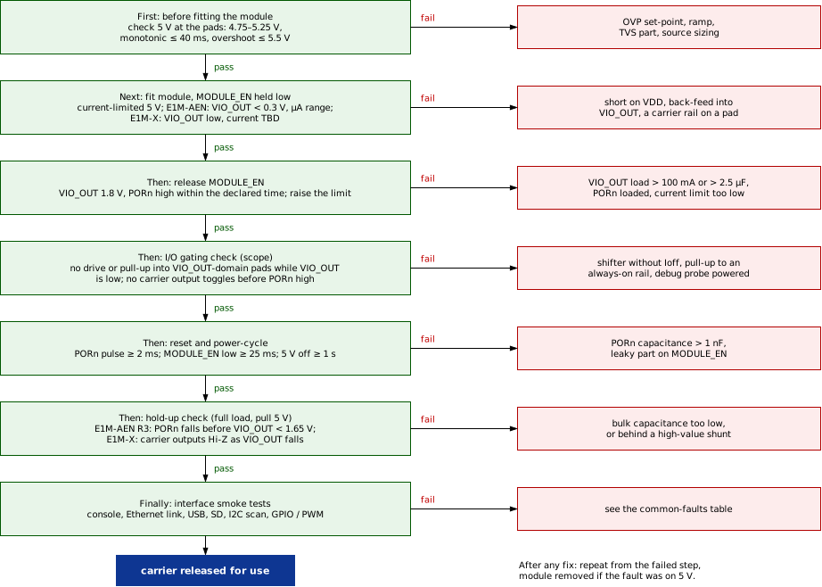
Bring-up order with pass and fail branches. The 5 V, VIO_OUT and PORn limits are the any-module values of E1M-STD-1.0 revision 1.4; the held-off values in the second step and the hold-up check are qualified per module family
23.1 Test points and bench set-up
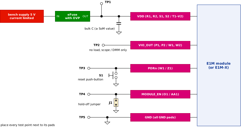
Recommended bring-up test points at the module pads, with the MODULE_EN hold-off jumper and the PORn reset button
| ID | Strength | Rule | Source |
|---|---|---|---|
| CB-BRU-01 | SHOULD | Provide test points next to the module pads for VDD / VDD_5V_IN (at the pads, after every series element), VIO_OUT, PORn, MODULE_EN and GND. A test point adds capacitance: keep the PORn total within 1 nF (CB-EMC-15). | Guide (informative); E1M-STD §6.3.1 (3) |
| CB-BRU-02 | SHOULD | Make MODULE_EN and PORn accessible: a jumper or switch from MODULE_EN to GND (hold-off), and a push-button from PORn to GND (reset). | HG-V2N-001 Design Checklist; HG-AEN-001 Power Bring-up on a New Carrier |
| CB-BRU-03 | MUST | Use a debug probe or console adapter only with VIO_OUT as its target reference and its target-power output disabled; its outputs stay high-impedance while VIO_OUT is low. | E1M-STD §6.2.3 (6) |
23.2 Before fitting the module
- First, inspect the bare carrier: footprint orientation (pad
A1against the carrier fiducial), solder-mask and paste openings, and no part inside the pad ring. - Next, power the carrier without a module and measure at the module pads:
VDD/VDD_5V_INbetween 4.75 V and 5.25 V at no load and at a load equal to the declared peak current (an electronic load on the pads);- the ramp from 0 V to 4.75 V: monotonic and within 40 ms;
- the overshoot at hot-plug of the 5 V source: never above 5.5 V;
- the fitted TVS and eFuse part numbers against the design.
- Then measure the other pads of the empty footprint:
VIO_OUT(P1,P2/W1,W2),SD_VDD/SD_VDD_OUT(AH10/AQ30) and everyVIO_OUT-domain pad must read 0 V. A voltage there means a carrier rail or pull-up that will back-feed the module. - Finally, check that every
RSVDpad is open (no continuity to any net) and that no supply reachesSD_VDD(AH10) unless the carrier is declared for E1M-AEN hw_rev R2 modules only (Annex E).
| ID | Strength | Rule | Source |
|---|---|---|---|
| CB-BRU-04 | MUST | Verify the 5 V window, ramp and overshoot at the module pads before the first module is fitted. | E1M-STD §6.1.1 (1)–(3); HG-AEN-001 Power Bring-up step 1 |
| CB-BRU-05 | MUST | Verify with the module absent that no carrier rail or pull-up puts a voltage on VIO_OUT, SD_VDD / SD_VDD_OUT or any VIO_OUT-domain pad. | E1M-STD §6.1.2 (2), §6.2.3 (1), §6.7.1 |
23.3 First power with the module
- First, fit the module and hold
MODULE_ENlow (jumper fitted). - Next, apply 5 V from a current-limited supply (E1M-AEN: 300 mA limit; E1M-X: TBD). Check that
VIO_OUTstays low (E1M-AEN: below 0.3 V, supply current in the microampere range; E1M-X V2N / V2N-M1:VIO_OUTlow, held-off current TBD, becauseMODULE_ENis pulled up toVDDINon the module and the shutdown current is not published). - Then release
MODULE_EN. Check thatVIO_OUTrises to 1.8 V and thatPORngoes high within the time the module declares (E1M-AEN: about 206 ms, at most 290 ms). Then raise the current limit to the module's source requirement (E1M-AEN ≥ 1.5 A; E1M-X ≥ 5 A). - Finally, check for abnormal heating of the module and of the carrier input stage (on V2N-M1, particularly over the DX-M1).
E1M-X V2N and V2N-M1 have no ready output and their hand-off delay is TBD (E1M-STD §6.2.1). Until it is published, treat VIO_OUT high and PORn high as the earliest point to drive pads, and confirm the boot on the console before you drive application interfaces.
| ID | Strength | Rule | Source |
|---|---|---|---|
| CB-BRU-06 | SHOULD | Apply the first 5 V with MODULE_EN held low and a current limit (E1M-AEN: 300 mA; E1M-X: TBD), and check that VIO_OUT stays low (E1M-AEN: < 0.3 V, μA-range current; E1M-X: VIO_OUT low, current TBD). Then release MODULE_EN and raise the limit only after VIO_OUT and PORn are high. | HG-AEN-001 Power Bring-up steps 2–3; Guide (informative) for E1M-X |
23.4 I/O gating check
Scope the busiest carrier lines into the module (UART RX, I2C, SPI, debug, every level-translator output) together with VIO_OUT and PORn, triggered on VIO_OUT:
- First at power-up: no carrier line may rise before
VIO_OUTis high, and no carrier output may toggle beforePORnis high. - Then at power-down: when
PORnfalls, every carrier output into the module must be high-impedance or low within 1 ms.
| ID | Strength | Rule | Source |
|---|---|---|---|
| CB-BRU-07 | MUST | Verify on a scope that no carrier circuit drives or pulls up a VIO_OUT-domain pad while VIO_OUT is low, and that carrier outputs are Hi-Z or low within 1 ms after PORn falls. | E1M-STD §6.2.2 (2), §6.2.3 (1), (3) |
E1M-AEN hw_rev R3 pulls PORn low before its 1.8 V rail falls (on-module supervisor; R2 has none, Annex E). Whether E1M-X V2N drives PORn low at power-down is not documented. On a carrier for E1M-X, verify that the carrier outputs also go Hi-Z when VIO_OUT falls.
23.5 Reset and power-cycle checks
- First, pull
PORnlow for ≥ 2 ms with the reset button: the SoC must restart, withVIO_OUTkept high. - Next, pull
MODULE_ENlow for ≥ 25 ms:PORnmust fall (E1M-AEN: about 1 ms after the falling edge) and the module must cold-boot on release. - Then switch 5 V off for ≥ 1 s and on again: the module must boot. On E1M-AEN, when
MODULE_ENis not wired (the "Always on" reference configuration), a 5 V cycle with at least 1 s off is the only restart after self-off if firmware armed no wake; withMODULE_ENwired, a low pulse ≥ 2 ms and release also wakes it. - Then, with firmware that supports it, check the standby entry and wake on
MODULE_STBY, and measure the standby current (E1M-AEN). - Finally, do the hold-up check under full load: on E1M-AEN R3, pull 5 V and check that
PORnfalls beforeVIO_OUTdrops below 1.65 V; on E1M-X, check that every carrier output into the module goes Hi-Z or low asVIO_OUTfalls (CB-BRU-09).
| ID | Strength | Rule | Source |
|---|---|---|---|
| CB-BRU-08 | SHOULD | Test reset (PORn ≥ 2 ms), forced power cycle (MODULE_EN low ≥ 25 ms) and a 5 V cycle with ≥ 1 s off on every carrier build. | E1M-STD §6.3.1 (3); DS-AEN-001 Control Timing, Reference Carrier Configurations |
| CB-BRU-09 | SHOULD | Hold-up check under full load. E1M-AEN R3: pull 5 V and check that PORn falls before VIO_OUT drops below 1.65 V; if it does not, the hold-up capacitance is too low or sits behind a high-value shunt. E1M-X V2N / V2N-M1 (no documented PORn behaviour at power-down): pull 5 V and check that every carrier output into the module is Hi-Z or low before VIO_OUT falls below 1.65 V. | HG-AEN-001 Power Bring-up step 7, Hold-up and Brownout; E1M-STD §6.2.3 (1) for E1M-X |
PORn low, MODULE_EN low and a 5 V cut give the module firmware no notice; a write to on-module non-volatile memory in progress at that moment is lost or corrupted.
23.6 Interface smoke tests
Add peripherals one at a time, in this order: console, Ethernet, USB, SD card, I2C devices, then display and camera.
| Interface | Test | Notes |
|---|---|---|
| Console | boot messages on the debug console (DBG_TX / DBG_RX) | adapter referenced to VIO_OUT (CB-BRU-03) |
| Ethernet | link on every routed port | E1M-AEN: one 100 Mbps port (ETH0); E1M-X: two 1 Gbps ports |
| USB | enumeration with a data-capable cable | power-only USB-C cables are common |
| SD card | card detect and a read / write | card supply comes from the module |
| I2C | bus scan | no carrier device at an on-module address (Chapter 19) |
| GPIO / PWM | toggle from a simple firmware build | only while VIO_OUT is high |
| Display, camera | panel image; sensor probe over I2C | set the panel I/O level before connecting; no hot-plug |
| DX-M1 (V2N-M1 only) | lspci shows PCIe 1ff4:0000; dxrt-cli -s returns rc 0; a first inference with run_model on the e1m-v2m10x-a55 image | the DX-M1 rail, reset and PCIe multiplexer are set up only by the Alp Lab U-Boot |
| ID | Strength | Rule | Source |
|---|---|---|---|
| CB-BRU-10 | MUST | On E1M-X V2N-M1, do not run a boot loader, M33 image, Linux tool or bench script that enables the DX-M1 rail or writes the on-module PMIC, other than the Alp Lab U-Boot or a replacement that implements its complete sequence. | DS-V2N-M1-001 Power Architecture; HG-V2N-M1-001 Boot |
| CB-BRU-11 | MUST | On E1M-X V2N-M1, do not flash stock DEEPX firmware to the DX-M1, and use the dxrt-cli options -u, -w and -C only with firmware that Alp Lab supplies for this module. | DS-V2N-M1-001 Boot Modes; HG-V2N-M1-001 DX-M1 model deployment |
A second PMIC writer or an out-of-order DX-M1 rail enable can bring the 0.75 V DX-M1 core rail up at the PMIC's 1.80 V default and damage the DX-M1.
Stock DEEPX firmware leaves the DX-M1 NPUs dead (dxrt_polling_ack: timeout); recovery needs a boot-strap change on the module and is not a field operation.
23.7 Common faults
| Symptom | Likely cause | Module |
|---|---|---|
Module never boots; VIO_OUT stays low | MODULE_EN held low: jumper fitted, leaky ESD part or pull-up to a switched rail on MODULE_EN, or an unpowered host pin clamping it | all |
| Module boots, then restarts at random | VDD dips below 4.75 V at load peaks (shunt, OR-ing diode, long leads); MODULE_EN leakage | all |
| Module boots on the bench, not in the product | 5 V source sized for the average current, not the peak; insufficient supply under PCIe SSD and AI load | all; E1M-X most often |
VIO_OUT not 1.8 V, or slow to rise | bulk capacitance or a heavy load on VIO_OUT; carrier rail back-feeding it | all |
PORn never rises or rises slowly | carrier pull-up on PORn, or total capacitance above 1 nF (for example a 100 nF debounce capacitor) | all |
| No boot on E1M-X | wrong boot DIP position on BOOT0 / BOOT1 (the most common first-time failure) | V2N, V2N-M1 |
| No console output | adapter not referenced to VIO_OUT; DBG_TX / DBG_RX crossed; wrong settings | all |
| Ethernet link down | magnetics missing or RJ-45 miswired; LED circuit loading a PHY strap pad | all |
| USB device not seen | power-only USB-C cable; CC terminated twice or not at all | all |
| SD card not seen | carrier supply on SD_VDD (AH10) on an R3 module; pull-ups to 3.3 V instead of the module supply | E1M-AEN |
| CAN silent | bus-level module on the default carrier-transceiver fit (E1M-STD §6.7.2 (3)); CAN_STBY left in standby | V2N, V2N-M1; E1M-AEN PHY option |
| High standby current | pull-ups or drivers on pads of switched on-module islands (E1M-AEN Wi-Fi pads); +S_CAP floating; leaky TVS | E1M-AEN |
| DX-M1 not enumerating | U-Boot did not bring up the DX-M1 rail, release its reset or route the PCIe multiplexer; image built for e1m-v2n10x-a55 instead of e1m-v2m10x-a55 | V2N-M1 |
| Wrong firmware | image built for another Ensemble variant (E1M-AEN) or another SKU / core | all |
23.8 Expected values per module
| Item | E1M-AEN | E1M-X V2N | E1M-X V2N-M1 |
|---|---|---|---|
| First-power current limit, then | 300 mA, then ≥ 1.5 A | TBD, then ≥ 5 A source | TBD, then ≥ 5 A source |
VIO_OUT with MODULE_EN held low | below 0.3 V, current in the μA range | low; current TBD (MODULE_EN pulled up to VDDIN on the module) | as V2N |
PORn high after 5 V or MODULE_EN release | 206 ms typical, 290 ms maximum | TBD (no ready output) | TBD (no ready output) |
| Debug console | DBG_TX AD3 / DBG_RX AE3: Alif Secure Enclave UART | DBG_TX AC62 / DBG_RX AD62 (E1M-STD §7.3.10); console function per manifest, TBD in the module documents (HG-V2N-001 names a SCIF console at 115 200 8N1, without its pads) | as V2N |
| Boot straps | not connected on the module | sampled at the rising edge of PORn; BOOT0 / BOOT1 boot device; BOOT2 fixed at 1; BOOT3 high = CA55, low = CM33 (carrier DIP circuit: Chapter 9) | as V2N |
| Standby currents | STOP 3.84 μA, self-off 1.14 μA, shutdown 2.94 μA (typical, calculated, 25 °C) | TBD | TBD |
| Extra checks | hw_rev R2 or R3 (Annex E); STOP and self-off wake | both Ethernet links | lspci 1ff4:0000; dxrt-cli -s rc 0; e1m-v2m10x-a55 image |
23.9 Chapter checklist
| ID | Check | Done |
|---|---|---|
| CB-BRU-01 | Test points at the pads for VDD, VIO_OUT, PORn, MODULE_EN, GND. | ☐ |
| CB-BRU-02 | MODULE_EN hold-off jumper and PORn reset button fitted. | ☐ |
| CB-BRU-03 | Debug probe: VIO_OUT reference, target power off. | ☐ |
| CB-BRU-04 | 5 V window, ramp and overshoot verified before the first module. | ☐ |
| CB-BRU-05 | No voltage on VIO_OUT, SD_VDD or VIO_OUT-domain pads with the module absent; RSVD pads open. | ☐ |
| CB-BRU-06 | First power with MODULE_EN low and a current limit. | ☐ |
| CB-BRU-07 | I/O gating verified on a scope at power-up and power-down. | ☐ |
| CB-BRU-08 | Reset, forced power cycle and 5 V cycle tested. | ☐ |
| CB-BRU-09 | Hold-up check under full load passed (E1M-AEN R3: PORn first; E1M-X: outputs Hi-Z). | ☐ |
| CB-BRU-10 | V2N-M1: only the Alp Lab U-Boot sequence touches the DX-M1 rail. | ☐ |
| CB-BRU-11 | V2N-M1: no stock DEEPX firmware flashed. | ☐ |
24 Carrier Conformance Checklist
This chapter collects, in one place, every carrier clause of the E1M specification (E1M-STD-1.0 revision 1.4) and the guide rules that a carrier needs to host any conformant module. Use it as the design-review record of a carrier: one copy per build variant.
24.1 How to use this checklist
- ID is the checklist row. Rows CB-CNF-01 to CB-CNF-10 are the ten carrier-conformance clauses of E1M-STD §9.2; rows from CB-CNF-11 on are the other carrier clauses of the specification.
- Clause is the E1M-STD clause that makes the row normative. Clause numbers follow the specification, for example "§6.1.1 (3)" is clause 3 of §6.1.1.
- Verify names the method: R review of schematic, layout or BOM; M measurement on the built carrier; I inspection of the assembled carrier.
- Applies says which form factor the row concerns: both, E1M-X (the row concerns pads that exist only on E1M-X), or variant (the row depends on the fit the build variant declares).
- Result is left empty for the reviewer. A carrier is E1M-conformant only when every row of §9.2 passes for its declared form factor.
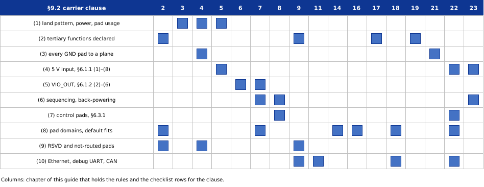
Traceability of the ten E1M-STD §9.2 carrier clauses to the chapters of this guide
24.2 Core conformance items (E1M-STD §9.2)
| ID | Clause | Requirement | Verify | Applies | Result |
|---|---|---|---|---|---|
| CB-CNF-01 | §9.2 (1), §5.1.1, §7.1 | The land pattern, the power delivery and the pad-by-pad signal usage match the chosen form factor's coordinate space. E1M: signal pads on a 1.0 mm grid, 0.40 mm round pads. Footprint and netlist checked pad by pad against pinout/v1.json (E1M) or pinout/x-v1.json (E1M-X); the EDA library keeps the pad letters I and O. | R | both | ☐ |
| CB-CNF-02 | §9.2 (2), §8.4 | No tertiary function is required, unless the carrier explicitly targets a single SoM or a declared set of SoMs in its BOM or build system. | R | both | ☐ |
| CB-CNF-03 | §9.2 (3), §7.3.1 | Every GND pad (49 on E1M, 105 on E1M-X) is connected to a low-impedance ground plane. | R, I | both | ☐ |
| CB-CNF-04 | §9.2 (4), §6.1.1 (1)–(8) | 5 V input: 4.75–5.25 V at the pads up to the declared peak current; ≤ 5.5 V at all times; monotonic ramp to 4.75 V within 40 ms; every VDD / VDD_5V_IN pad connected (R1, R2, S1, S2 / T1, T2, U1, U2, V1, V2) and no other supply on them; source sized for the peak current; over-voltage and (where needed) reverse-polarity protection; bulk capacitance ≥ the declared value; no back-feeding by OR-ing, ≥ 4.75 V still at the pads. | R, M | both | ☐ |
| CB-CNF-05 | §9.2 (5), §6.1.2 (2)–(6) | VIO_OUT (P1, P2 / W1, W2): never driven or tied to another rail; used only as translator reference and pull-up rail, module-on indication or load-switch enable; total load ≤ 100 mA, ≤ 50 mA in the first 2 ms, ≤ 2.5 μF; translators Hi-Z with their VIO_OUT side off; monitors cannot back-power an unpowered host. | R, M | both | ☐ |
| CB-CNF-06 | §9.2 (6), §6.2.1–§6.2.3 | Pads driven only after VIO_OUT high and PORn high; outputs Hi-Z or low within 1 ms after PORn falls; no drive or pull-up into VIO_OUT-domain pads while VIO_OUT is low; pull-ups only to VIO_OUT or a rail it switches; pads kept within −0.3 V to 1.98 V; debug probes referenced to VIO_OUT with target power off; declared switched pad groups respected. | R, M | both | ☐ |
| CB-CNF-07 | §9.2 (7), §6.3.1 (1)–(4) | MODULE_EN pulled low only by open drain, switch or button, no pull-up to a rail that can be off, buffered from a host that can be unpowered, every part rated 5.5 V, leakage ≤ 0.1 μA; MODULE_STBY open drain, no pull-up above VIO_OUT, leakage ≤ 0.1 μA; PORn open drain, never driven high, no pull-up, low pulse ≥ 2 ms, ≤ 1 nF; JTAG_nRST open drain, pull-up only to VIO_OUT. | R, M | both | ☐ |
| CB-CNF-08 | §9.2 (8), §6.7.1, §6.7.2 | Pads outside the VIO_OUT domain are never clamped, pulled up or translated as 1.8 V signals; the default assembly of every dual-meaning pad group is the fit that cannot damage any conformant SoM (CAN: carrier-transceiver path fitted, bypass not fitted); the two CAN paths are never both fitted; each build variant declares its fits and its supported SoMs. | R | variant | ☐ |
| CB-CNF-09 | §9.2 (9), §7.3.3, §7.3.4 | Every RSVD pad (34 on E1M, 20 on E1M-X) left unconnected: no trace, test point, pull resistor, load or jumper. No unrelated net routed through a pad that a SoM does not route; only spec NC pads (E1M-X only) may carry other nets. | R, I | both | ☐ |
| CB-CNF-10 | §9.2 (10), §7.3.6, §7.3.10, §7.3.14 | Ethernet, debug UART and CAN carrier clauses met (rows CB-CNF-16 to CB-CNF-18). | R | both | ☐ |
24.3 Other specification clauses for carriers
| ID | Clause | Requirement | Verify | Applies | Result |
|---|---|---|---|---|---|
| CB-CNF-11 | §6.1 | SHOULD: additional decoupling close to high-current loads on the carrier side. | R | both | ☐ |
| CB-CNF-12 | §6.3 | MAY: MODULE_EN, MODULE_STBY and PORn left unconnected; the carrier then needs no pull-up on any of them, and the module boots on 5 V. | R | both | ☐ |
| CB-CNF-13 | §6.4 | BOOT2 driven to the SoM manifest's declared default, or left to the SoM's internal pull. | R | both | ☐ |
| CB-CNF-14 | §6.5 | No external Ethernet PHY, Wi-Fi/BLE module or CAN transceiver between the carrier and these signal classes, except the transceiver for a CAN group that the SoM declares as logic-level CAN. | R | both | ☐ |
| CB-CNF-15 | §7.3.2 | Antenna trace 50 Ω where used; ANT_* pads the module does not drive left unconnected (a not-fitted link at the pad meets this for a carrier that hosts any module). | R, I | variant | ☐ |
| CB-CNF-16 | §7.3.6 (1)–(4) | Magnetics or a transformer-integrated RJ-45 for each used port, no external PHY; every MDI pair routed as 100 Ω differential; all four pairs of every used port routed to magnetics rated for 1000BASE-T; MDI ESD between magnetics and connector (discrete magnetics) or on the PHY side at the jack (transformer-integrated RJ-45, Annex C, C-31); no extra pull resistors on ETHx_LED0 / ETHx_LED1, LEDs only as the manifest declares. | R, I | both | ☐ |
| CB-CNF-17 | §7.3.10 | DBG_RX (AE3 / AD62) driven only while VIO_OUT is high. SHOULD: DBG_TX / DBG_RX brought to a header or to a USB-to-UART bridge referenced to VIO_OUT. | R, M | both | ☐ |
| CB-CNF-18 | §7.3.14 | No CAN bus, terminator or bus-side protection directly on a CAN pad unless every declared SoM implements that group as bus-level CAN; carrier transceiver (logic-level groups) with its logic supply from VIO_OUT or a rail it switches, logic pins Hi-Z when unpowered; CAN_STBY (A19 / A21) never pulled low, and driven only where the manifest declares it a SoM input. | R | variant | ☐ |
| CB-CNF-19 | §8.2 | A pad used as GPIO stays compatible with a SoM that routes only the default function; GND, NC, RSVD, POWER_*, ANT_*, BL_LED_A and BL_LED_K are never used as GPIO. | R | both | ☐ |
| CB-CNF-20 | §8.3 | JTAG / SWD compound pads (JTAG_TCK/SWDCLK, JTAG_TMS/SWDIO): either function may be selected. CAN compound pads: the reading fixed by the SoM's declared CAN option is used. | R | variant | ☐ |
| CB-CNF-21 | §5.2, §5.3 | Mounting per the E1M-STD-1.0 revision 1.5 §5.2 rule (spacer PCB soldered on both faces, or carrier cut-out), with no carrier components inside the cavity outline; any EMI shield on the SoM stays within the module height envelope (no carrier part above the module). | R | both | ☐ |
| CB-CNF-22 | §5.4 | The carrier assembly process uses LGA-class reflow (Chapter 3). | R | both | ☐ |
| CB-CNF-23 | §6.2.2 (1), (4) | SHOULD: a graceful shut-down request path exists; 5 V is removed only after VIO_OUT is low. | R | both | ☐ |
| CB-CNF-24 | §7.3 (E1M-X pads) | Interfaces that exist only on E1M-X (PCIE1_*, CSI2_*, CSI3_*, LCD_*, USB1_30_*, I2C2_*, I2C3_*, SPI2_*, CAN1, +V_CAM2, +V_CAM3) are not checked on an E1M carrier. | R | E1M-X | ☐ |
24.4 Guide-level items (roll-up)
Each chapter of this guide ends with its own checklist. A carrier that hosts any module passes every MUST row of every chapter checklist below; SHOULD rows that are not met are recorded with the reason.
| Chapter | Area | Result |
|---|---|---|
| 2 | Designing for any module: unrouted pads, option resistors, forbidden pads | ☐ |
| 3 | Footprint, mechanics and assembly | ☐ |
| 4 | PCB stack-up and controlled-impedance routing | ☐ |
| 5 | 5 V input stage | ☐ |
| 6 | Module output rails | ☐ |
| 7 | I/O levels, level shifting and back-powering | ☐ |
| 8 | Control pins, module states and power sequencing | ☐ |
| 9 | Boot configuration and debug access | ☐ |
| 10 | RTC backup store (+S_CAP) | ☐ |
| 11 | Ethernet | ☐ |
| 12 | Wi-Fi / Bluetooth antenna | ☐ |
| 13 | USB | ☐ |
| 14 | SD card / SDIO | ☐ |
| 15 | Camera interfaces | ☐ |
| 16 | Display interfaces and backlight | ☐ |
| 17 | PCIe | ☐ |
| 18 | CAN | ☐ |
| 19 | I2C, I3C, UART, SPI, I2S and PDM | ☐ |
| 20 | ADC, DAC, PWM, encoder and GPIO | ☐ |
| 21 | Thermal design (CB-THM-01 to CB-THM-13) | ☐ |
| 22 | EMC and ESD protection (CB-EMC-01 to CB-EMC-21) | ☐ |
| 23 | Carrier bring-up (CB-BRU-01 to CB-BRU-11) | ☐ |
24.5 Module-targeted carriers: declaring a SoM set
A carrier MAY depend on a tertiary function, use a wider 5 V window, fit the CAN bypass path or omit a protection that a particular module provides, but only when it declares the set of SoMs it supports (E1M-STD §9.2 (2), §6.1.1, §6.7.2 (3), (5)). The declaration lives in the carrier's BOM and build system, so that a module outside the set is rejected before it is fitted or flashed.
| Item | Content |
|---|---|
| Build variant | carrier name, PCB revision and BOM variant name |
| Form factor | E1M or E1M-X |
| Supported SoMs | SKUs and hardware revisions (for example E1M-AEN801 hw_rev R3; E1M-V2N101 to E1M-V2N103) |
| Dual-meaning pad fits | for each group: CAN (carrier transceiver or bypass, per CAN group), and any other assembly option of the carrier (antenna feeds, USB D± group, backlight path, +S_CAP store) |
| Tertiary functions | each tertiary function used, its pad, and the SoMs whose manifest exposes it |
| Wider limits used | any limit wider than the any-module value (for example the 5 V window), with the manifest values that allow it |
| Temperature range | the product ambient range the carrier is qualified for |
24.6 Per-module differences
| Item | E1M-AEN | E1M-X V2N | E1M-X V2N-M1 |
|---|---|---|---|
| CAN option | standard build: logic-level CAN on CAN0; on-module transceiver as an assembly option (bus-level) | bus-level CAN on CAN0 and CAN1 (transceivers populated by default) | as V2N |
| Ethernet | one 100 Mbps port (ETH0); PHY-internal MDI ESD | two 1 Gbps ports; no on-module MDI ESD | as V2N |
| Boot straps | BOOT0–BOOT3 not connected on the module; strap declared ignored (§6.4 (3)) | BOOT0 / BOOT1 select the boot device; BOOT2 fixed at 1; BOOT3 boot CPU | as V2N |
| Debug console | DBG_TX / DBG_RX = Alif Secure Enclave UART | DBG_TX / DBG_RX = on-module debug UART | as V2N |
| PCIe | not routed | PCIE0, Gen3 × 2 | PCIE0 shared with the on-module DX-M1 |
| Wi-Fi bands | 2.4 GHz only; AF1, AD1 not connected and declared (§6.5) | 2.4 / 5 / 6 GHz radio; the pin table routes only AR1 (Annex C, C-35) | as V2N |
| Open conformance points against E1M-STD-1.0 revision 1.4 | no height class declared (C-34). The ignored boot strap and the 2.4 GHz-only radio are conformant in revision 1.4 (C-05, C-10) | BOOT2 "Not connected" in the pin table against the §6.4 strap (C-06); only AR1 routed, with the bands on AR1 and the unused AP1 / AN1 not yet declared (§6.5, §7.3.2, C-35); no height class declared (C-34); values marked TBD (Annex C) | as V2N, plus PCIE0 and some IOs owned by the on-module DX-M1 (C-22) |
24.7 Chapter checklist
| ID | Check | Done |
|---|---|---|
| CB-CNF-01 to 10 | All ten §9.2 rows pass for the declared form factor. | ☐ |
| CB-CNF-11 to 24 | All other specification rows pass or are marked not applicable with a reason. | ☐ |
| Roll-up | Every MUST row of chapters 2 to 23 passes. | ☐ |
| Declaration | Each build variant declares its form factor, SoM set, dual-meaning pad fits, tertiary functions and wider limits. | ☐ |
| Record | This checklist is filed with the carrier design release, one copy per build variant. | ☐ |
Annexes
The annexes are informative. The pad data comes from the published pinout files pinout/v1.json (E1M, 312 pads) and pinout/x-v1.json (E1M-X, 496 pads) of E1M-STD-1.0 revision 1.4; the module values come from the module datasheets and hardware design guides. Where a module document and the specification differ, Annex C records the issue and the way this guide handles it.
Annex A (informative): Carrier pad quick reference
Pad maps by carrier rule class
The two maps below colour every pad by the rule that governs it on the carrier. The orientation is the pad frame of Chapter 1 (the frame of the alplab.ai pinout viewer): top view, pad A1 at the top left, letters on the rows (top to bottom), numbers on the columns (left to right); E1M-X is landscape.
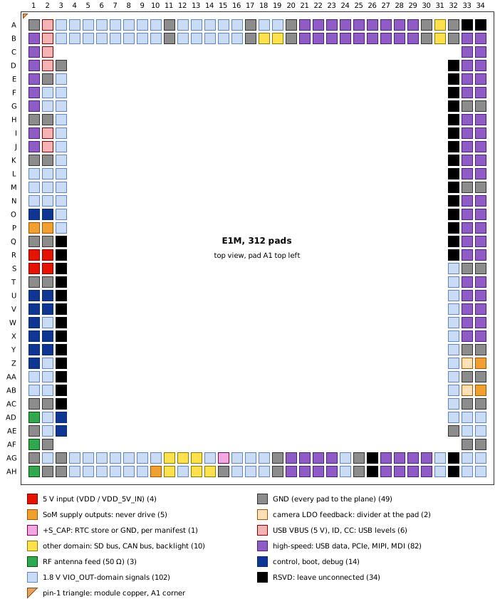
E1M pad map by carrier rule class (top view), with the pad count of each class
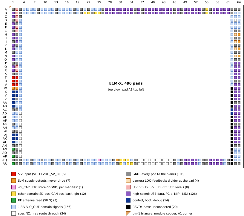
E1M-X pad map by carrier rule class (top view), with the pad count of each class
The classes follow E1M-STD §6.7.1. Only SD_CLK, SD_CMD, SD_D0–SD_D3, the CAN bus pads and BL_LED_A / BL_LED_K are drawn as "other domain"; SD_DET, SD_RST and CAN_STBY are VIO_OUT-domain (1.8 V) pads. The CAN bus pads carry bus-level or 1.8 V logic signals depending on the CAN option the module declares (§6.7.2). +S_CAP gets the RTC backup store or a tie to GND as the manifest declares, never left floating on E1M-AEN (Chapter 10). CAM_VFBx are feedback inputs: fit the divider at the pad (Chapter 15). USB VBUS pads carry 5 V. RSVD pads (black) are left unconnected on every carrier (§7.3.3). Only spec NC pads (white, E1M-X only) may carry other carrier nets (§7.3.4); a pad that one module leaves unrouted keeps its standard function on other modules.
Carrier-relevant pads
| Signal (silkscreen) | E1M | E1M-X | Carrier rule |
|---|---|---|---|
VDD (E1M) / VDD_5V_IN (E1M-X) | R1, R2, S1, S2 | T1, T2, U1, U2, V1, V2 | 5 V input, E1M-STD §6.1.1; Chapter 5 |
GND | 49 pads (pinout/v1.json) | 105 pads (pinout/x-v1.json) | every pad to a ground plane, §9.2 (3) |
VIO_OUT | P1, P2 | W1, W2 | SoM output, §6.1.2; Chapter 6 |
MODULE_EN | O1 | AA1 | 5 V tolerant, open drain, §6.3.1 (1) |
MODULE_STBY | O2 | AB1 | open drain, §6.3.1 (2) |
PORn | W1 | Z1 | open drain, no pull-up, ≤ 1 nF, §6.3.1 (3) |
BOOT0, BOOT1, BOOT2, BOOT3 | V2, U2, U1, V1 | Y2, X2, X1, Y1 | per SoM manifest, §6.4; Chapter 9 |
JTAG_TCK/SWDCLK, JTAG_TDI, JTAG_TDO, JTAG_TMS/SWDIO, JTAG_nRST | X1, X2, Y2, Y1, Z1 | AJ1, AJ2, AK2, AK1, AL1 | 1.8 V; probe referenced to VIO_OUT, §6.2.3 (6); JTAG_nRST open drain, §6.3.1 (4) |
DBG_TX, DBG_RX | AD3, AE3 | AC62, AD62 | debug console, §7.3.10 |
+S_CAP | AG15 | AQ25 | RTC backup store, per manifest; Chapter 10 |
RTC_CLKOUT | AH16 | AQ16 | 32 kHz output |
SD_VDD (E1M) / SD_VDD_OUT (E1M-X) | AH10 | AQ30 | SoM output; never a carrier supply, §6.7.1 |
+V_CAM0, +V_CAM1 | Z34, AB34 | H64, J64 | SoM outputs; Chapter 15 |
+V_CAM2, +V_CAM3 | (E1M-X only) | L64, N64 | SoM outputs; Chapter 15 |
CAM_VFB0, CAM_VFB1 | Z33, AB33 | H63, J63 | feedback divider at the pad |
CAM_VFB2, CAM_VFB3 | (E1M-X only) | L63, N63 | feedback divider at the pad |
BL_LED_A, BL_LED_K | A31, B31 | B55, A55 | LED string only (up to 36 V on E1M-AEN), §6.7.1 |
ANT_2.4GHZ, ANT_5GHZ, ANT_6GHZ | AH1, AF1, AD1 | AR1, AP1, AN1 | 50 Ω; undriven pads unconnected, §7.3.2 |
CAN0H/CAN0_TX, CAN0L/CAN0_RX | B18, B19 | B21, B22 | per declared CAN option, §6.7.2, §7.3.14 |
CAN1H/CAN1_TX, CAN1L/CAN1_RX | (E1M-X only) | B24, B25 | per declared CAN option |
CAN_STBY | A19 | A21 | never pulled low, §7.3.14 |
I2C0_SCL, I2C0_SDA | AE2, AD2 | AH1, AH2 | on-module devices on the bus; Chapter 19 |
RSVD | A33, A34, D32–P32, Q32, R32, Q3–AC3, AG26, AG32, AH26, AH32 (34 pads) | W62–AB62, AE62–AR62 (20 pads) | leave unconnected, §7.3.3 |
NC | none | D63, AD3–AP3, AQ36–AQ45, AR36–AR45 (34 pads) | MAY route through, §7.3.4 |
Same pad name, different signal
The two form factors use independent coordinate spaces (E1M-STD §7.1). The same pad name carries a different signal on the other form factor, often a power or control pad. Never copy a footprint, a netlist or a pad-assignment table from one form factor to the other by pad name.
| Pad | E1M | E1M-X | Consequence if copied |
|---|---|---|---|
R1, R2 | VDD | USB1_30_TX0_N, USB1_30_ID | 5 V on USB pads |
S1, S2 | VDD | GND | 5 V shorted to ground |
T1, T2 | GND | VDD_5V_IN | 5 V input shorted to ground |
U1, U2, V1, V2 | BOOT2, BOOT1, BOOT3, BOOT0 | VDD_5V_IN | boot-strap circuit on the 5 V input |
P1, P2 | VIO_OUT | GND | VIO_OUT shorted to ground |
W1 | PORn | VIO_OUT | reset circuit on the I/O rail |
W2 | IO2 | VIO_OUT | a pull-up or drive on IO2 back-feeds or loads the E1M-X VIO_OUT |
Z1 | JTAG_nRST | PORn | debug reset wired to the module reset |
X1, X2, Y1, Y2 | JTAG / SWD | BOOT2, BOOT1, BOOT3, BOOT0 | debug lines on boot straps |
O1, O2 | MODULE_EN, MODULE_STBY | USB1_30_RX0_N, IO3 | control circuits on signal pads |
AA1, AB1 | PDM_C0, PDM_C1 | MODULE_EN, MODULE_STBY | microphones on the control pads |
A19 | CAN_STBY | DAC0 | transceiver standby on a DAC output |
B18, B19 | CAN0H/CAN0_TX, CAN0L/CAN0_RX | GND, DAC1 | CAN on ground and a DAC |
A21 | PCIE0_TX0_P | CAN_STBY | PCIe lane AC-coupling or termination on the transceiver standby pad |
B21, B22 | PCIE0_TX0_N, PCIE0_TX1_N | CAN0H/CAN0_TX, CAN0L/CAN0_RX | bus voltage on PCIe lanes |
B24, B25 | PCIE0_TX3_N, PCIE0_RX0_N | CAN1H/CAN1_TX, CAN1L/CAN1_RX | bus voltage on PCIe lanes |
A31, B31 | BL_LED_A, BL_LED_K | PCIE1_RX0_P, PCIE1_RX0_N | backlight voltage (up to 36 V) on PCIe lanes |
AD1, AF1, AH1 | ANT_6GHZ, ANT_5GHZ, ANT_2.4GHZ | SPI0_MISO, SPI0_CS1, I2C0_SCL | RF network on logic pads |
Q3–AC3 | RSVD | LCD_B13–LCD_B23, LCD_HSYNC, LCD_VSYNC | nets on reserved pads |
AD3, AE3 | DBG_TX, DBG_RX | NC | console lost |
Annex B (informative): Module capability and difference matrix
This matrix is the single source of the per-module values used in the chapters of this guide. Values are copied from the module documents; TBD means the module document does not state the value.
| Item | E1M-AEN | E1M-X V2N | E1M-X V2N-M1 |
|---|---|---|---|
| Form factor | E1M, 35 × 35 mm, 312 pads | E1M-X, 45 × 65 mm, 496 pads | E1M-X, 45 × 65 mm, 496 pads |
| Silicon | Alif Ensemble E3–E8 | Renesas RZ/V2N R9A09G056N44GBG#AC0 | RZ/V2N R9A09G056N44GBG#AC0 + DeepX DX-M1 |
| SKUs | E1M-AEN301, 401, 501, 601, 701, 801, 803 | E1M-V2N101, E1M-V2N102, E1M-V2N103 | E1M-V2M101, E1M-V2M102, E1M-V2M103 |
| Hardware revision | R3 (DS-AEN-001); R2 differences in Annex E | held in the identity EEPROM; not stated in the datasheet | as V2N |
| 5 V operating range | 4.75 / 5.0 / 5.25 V | 4.5 / 5.0 / 5.5 V (HG: ±5 % recommended) | 4.5 / 5.0 / 5.5 V (HG: ±5 %) |
| 5 V absolute maximum | 5.5 V | 6.0 V | 6.0 V |
| 5 V ramp | monotonic, 0 V to 4.75 V within 40 ms | not specified | not specified |
| Peak input current; source | 834 mA (E1M-AEN801, calculated) plus carrier loads; source ≥ 1.0 A continuous, ≥ 1.5 A peak | TBD; source ≥ 5 A | TBD; source ≥ 5 A |
| Carrier bulk capacitance | ≥ 50 μF effective per A of VDDIN load; about 50 μF on the module | ≥ 10 μF + 100 nF | ≥ 10 μF + 100 nF |
VIO_OUT | 1.8 V; ≤ 100 mA; ≤ 50 mA in the first 2 ms; ≤ 2.5 μF | 1.8 V ±5 %; current TBD | as V2N |
PORn high after power-up | 206 ms typical, 290 ms maximum | TBD; no ready output | TBD; no ready output |
MODULE_EN | 5 V tolerant; 1.0 ms glitch filter; pulses below 0.5 ms ignored; ≥ 25 ms low = full power cycle | pulled up to VDDIN on the module | as V2N |
MODULE_STBY | active low; 5 V tolerant; pulse or level protocol; self-off wake ≥ 10 ms | standby request to the GD32; RTC-only standby (reference firmware) | as V2N |
PORn reset pulse | ≥ 2 ms | TBD | TBD |
| Boot straps | not connected; strap declared ignored (§6.4 (3)) | BOOT0 / BOOT1 boot device; BOOT2 fixed at 1; BOOT3 boot CPU | as V2N |
| Ethernet | TI DP83825, 100 Mbps, ETH0 only | 2 × Realtek RTL8211FI-VD-CG, 1 Gbps | as V2N |
| Wi-Fi / BLE | TI CC3501E (BDE-BW3501N), 2.4 GHz only; ANT_5GHZ, ANT_6GHZ not connected | Murata LBEE5HY2FY (Infineon CYW55513), 2.4 / 5 / 6 GHz | as V2N |
| USB | USB 2.0 only, on B1 / C1 / C2 / D2 (R3) | USB 3.2 Gen 2 (host only, DS) on USB0_30_*; USB 2.0 on USB2_20_*; USB1_30_* not routed | as V2N |
| MIPI CSI-2 | CSI0, 2 lanes | 2 × 4 lanes | 2 × 4 lanes |
| MIPI DSI | DSI0, 2 lanes | 4 lanes (DS: one interface; HG: two) | as V2N |
| PCIe | not routed | Gen3 × 2 on PCIE0 | PCIE0 shared with the on-module DX-M1 |
| CAN | logic-level CAN0 (standard build); TCAN1044AVDRBRQ1 assembly option (bus-level) | 2 × bus-level (TCAN1044AVDRBRQ1, populated by default per HG) | as V2N |
| SD-card supply | SD_VDD 3.4 V output, switched by firmware | SD_VDD_OUT 1.8 / 3.3 V automatic, 300 mA | as V2N |
| Camera LDOs | 2 × 0.6–3.1 V, 170 mA combined, 100 mA per rail at 3.1 V | 4 × 0.6–3.3 V, 300 mA max each (DS pin table, H64, J64, L64, N64) | as V2N |
| Backlight | on-module driver; BL_LED_A up to 36 V; feedback voltage under review (Annex C) | on-module driver, up to 10 LEDs in series or 2P6S; ILED = 95 mV / RFB | as V2N |
RTC backup (+S_CAP) | RV-3028; carrier store; 15 kΩ charger to 3.05 V (supercap only); runs from the store above 2.0 V (2.2 V worst case) | on-module RTC; charger behaviour not documented | as V2N |
| On-module I2C addresses | identity EEPROM 0x50 / 0x58 on I2C0 | ACT88760 0x25 / 0x26, DA9292 0x1E (bus not stated) | as V2N |
| Operating ambient | −40 to +75 °C | −40 to +85 °C | −40 to +85 °C |
| Pad ESD (HBM / CDM) | ± 2000 V / ± 250 V | TBD | TBD |
Annex C (informative): Specification and module documentation issues
| ID | Issue | Status | Handling in this guide |
|---|---|---|---|
| C-01 | E1M-AEN standard build has no CAN transceiver (B18 / B19 are 1.8 V logic) against the bus-level CAN rule; Annex A.1 said every SKU carries TCAN1044AVDRBRQ1. | resolved in 1.3 (§6.5 logic-level CAN option; Annex A.1 corrected) | carrier-transceiver path is the default fit (§6.7.2) |
| C-02 | §8.3 let the carrier pick either CAN reading; §6.5 cited §7.3.13 for CAN. | resolved in 1.3 (§8.3; reference now §7.3.14) | — |
| C-03 | VIO_OUT level, current, tolerance and capacitance were not specified. | partly resolved in 1.3 (§6.1.2); E1M-X current and capacitance TBD | AEN limits applied to every module |
| C-04 | Both modules put their debug UART on pads listed as RSVD. | resolved in 1.3 (DBG_TX / DBG_RX at AD3 / AE3 and AC62 / AD62, §7.3.10) | Chapter 9 |
| C-05 | E1M-AEN leaves BOOT0–BOOT3 unconnected, against §6.4 and §9.1 (4). | resolved in 1.3 (§6.4 (1), (3), §9.1 (4): every SoM exposes the strap pads and a SoM may ignore them if its manifest declares it; E1M-AEN is conformant) | carrier keeps the strap circuit; no effect on a module that ignores the strap (Chapter 9) |
| C-06 | DS-V2N-001: BOOT2 "fixed at 1" in the boot section, "Not connected. Leave floating." in the pin table (X1). | open (module documentation) | leave BOOT2 to the module pull (CB-CNF-13) |
| C-07 | RTC_WAKE_N (E1M-AEN P3 = IO25) has no specification pad or signal kind. | resolved in 1.3 (alternate function of IO25, E1M P3 / E1M-X F63, §8.2; unchanged in 1.4) | Chapter 8; the E1M-AEN manifest still has to declare P3 as open drain up to 5.5 V |
| C-08 | Ethernet "post-magnetics" wording, "1 GbE" on a 100 Mbps module. | resolved in 1.3 (§6.5, §7.3.6) | Chapter 11 |
| C-09 | E1M-X Ethernet pair order in the Typst specification differed from DS-V2N-001 and pinout/x-v1.json. | resolved in 1.3 (for example ETH0_DA_N AR59, ETH0_DD_N AR56) | use the JSON |
| C-10 | §6.5 and §7.3.2 required 5 GHz; E1M-AEN is 2.4 GHz only. | resolved in 1.3 (§6.5, §7.3.2: 2.4 GHz required, 5 GHz and 6 GHz optional and declared; unused ANT_5GHz / ANT_6GHz no-connect and declared; E1M-AEN is conformant) | not-fitted link on the 5 GHz and 6 GHz pads (Chapter 12) |
| C-11 | Land pattern: E1M pitch now 1.0 mm with 0.40 mm pads. E1M-X pitch and pad size, tolerances, mask and paste openings are not yet published. | partly resolved: E1M pitch and pad size in 1.3 (§5.1.1); recommended carrier land pattern for both form factors in 1.4 (§5.1.3, informative, E1M-AEN values); E1M-X pitch and pad size not normative, tolerances and footprint library not specified in 1.4 or 1.5; E1M-X land pattern published in DS-V2N-001 0.10 and DS-V2N-M1-001 0.13 (1.00 mm pitch, ⌀ 0.40 mm NSMD pads, ⌀ 0.50 mm mask opening, 1:1 stencil) | Chapter 3 |
| C-12 | GND, NC, RSVD and GPIO counts in the specification prose did not match the JSON. | resolved in 1.3 (49 / 105 GND; 34 / 20 RSVD; 34 NC; 23 GPIO on E1M) | — |
| C-13 | No 5 V window, ramp, current or absolute maximum in the specification. | resolved in 1.3 (§6.1.1) | Chapter 5 |
| C-14 | No sequencing or back-powering rules; E1M-X hand-off delay and PORn behaviour at power-down not documented. | rules resolved in 1.3 (§6.2); E1M-X values open | gate on VIO_OUT and PORn (Chapter 23) |
| C-15 | MODULE_EN pull-up rail and MODULE_STBY polarity were undefined. | resolved in 1.3 (§6.3, §6.3.1) | parts on MODULE_EN rated 5.5 V |
| C-16 | DS-AEN-001: MODULE_EN pulses shorter than about 21 ms keep the SoC supply up; both AEN documents give ≥ 25 ms for a full power cycle. The 21–25 ms behaviour is not stated. | open (module documentation) | use ≥ 25 ms |
| C-17 | +S_CAP direction, voltage and charger control are not in the specification; the E1M-X charger is not documented. | open (manifest only) | Chapter 10 |
| C-18 | Backlight feedback voltage: HG-AEN-001 gives ILED = 200 mV / RFB, DS-AEN-001 and the V2N documents 95 mV / RFB. No R_FB location on V2N. | open | Chapter 16 |
| C-19 | USB: VBUS direction, ID function and CC ownership undefined; V2N USB 3 impedance 85 Ω (HG) against 90 Ω (DS); host only (DS) against host or function (HG); naming USB2_* / USB2_20_*. | open | Chapter 13 |
| C-20 | Specification Annex A.1 says E1M-AEN uses USB2_*; DS-AEN-001 (R3) puts USB 2.0 on B1 / C1 / C2 / D2 (USB0_30_* pads), with I1, J1, I2, J2 not connected. | open | Chapter 13 |
| C-21 | DSI count on V2N: HG-V2N-001 two 4-lane interfaces, DS-V2N-001 one. | open (module documentation) | Chapter 16 |
| C-22 | PCIe: no PERST# / CLKREQ# / WAKE# pads or reference-clock direction; on V2N-M1 PCIE0 and some IOs are owned by the DX-M1, against "reuse the V2N carrier without changes". | open | Chapter 17 |
| C-23 | LCD (E1M-X) has no pixel clock or DE pad; parallel camera data starts at CAM_D1. | open | Chapters 15, 16 |
| C-24 | Camera supply range and current, and the V2N feedback current, are not specified. | open | Chapter 15 |
| C-25 | Stale cross-references in HG-V2N-001 and HG-V2N-M1-001 (for example "HG-V2N-M1-001 §6.7", DS reflow and mechanical section numbers). | open (module documentation) | this guide cites section names |
| C-26 | Pad frame. The pinout JSON and the alplab.ai pinout viewer use letters as rows (down) and numbers as columns (across), E1M-X 65 mm across and 45 mm down. The footprint drawings (§5.1), placement areas (§5.3) and pad maps (§7.1) of E1M-STD-1.0 revisions 1.3 and 1.4 draw the letters across, and §7.1 calls the letters "columns". | addressed in 1.5 (draft) | figures, pad maps and frame text of this guide in the pad frame of Chapter 1 |
| C-27 | V2N and V2N-M1 datasheets do not state a hardware revision. | open (module documentation) | Annex E |
| C-28 | V2N-M1 cooling threshold: "∼50 % DX-M1 utilisation at +25 °C ambient" (Thermal) against "at the high end of the temperature range" (Environmental). | open (module documentation) | CB-THM-12 uses the threshold without an ambient |
| C-29 | E1M-X on-module PMIC addresses (0x1E, 0x25, 0x26) are given without their I2C bus. | open | keep these addresses free on every carrier I2C bus of an E1M-X carrier (Chapter 19) |
| C-30 | §5.1.2 referred to images/e1m-x-footprint.svg, which was not in the specification images. | resolved in 1.3 (drawing added) | — |
| C-31 | §7.3.6 (2) places the MDI ESD array "between the magnetics and the connector", while §7.3.6 also allows a transformer-integrated RJ-45, which has no accessible point there. The 2641-R3 carrier (HR851178A) has its arrays (D35, D39, D40, D41) on the PHY side, with the pairs running straight from the pads to the connector. | open (specification) | CB-EMC-05: discrete magnetics between magnetics and jack; integrated magnetics on the PHY side at the jack, rated for every hosted module's MDI |
| C-32 | 2641-R3 fits C1 1 nF on PORn at reset button S1, which uses the whole §6.3.1 (3) budget; with an ESD diode or a test point the node exceeds 1 nF. | open (EVK) | CB-EMC-15 counts the capacitor in the budget; no capacitor on new designs |
| C-33 | pinout/x-v1.json gave AQ62 and AR62 the silkscreen RVSD (typo for RSVD). | resolved in 1.3 (silkscreen now RSVD) | — |
| C-34 | §5.2 requires a height-class declaration; only HG-V2N-M1-001 declares one (standard height). DS-AEN-001 and DS-V2N-001 declare none. Alp Lab has replaced the height classes with two mounting options, a spacer PCB or a carrier cut-out at the module cavity (19 October 2026); the specification and the module documents do not state them yet, and spacer thickness, module height and bottom-side component height stay TBD. | open (specification and module documentation) | CB-MEC-09: spacer PCB or cut-out on every carrier; CB-THM-13: leave margin, confirm with Alp Lab |
| C-35 | DS-V2N-001 lists only AR1 as an antenna output (ANT_2.4GHz / NC; AP1, AN1 "leave floating") although the radio covers three bands; the V2N and V2N-M1 manifests do not yet declare which bands are on AR1 or that AP1 / AN1 are unused (§6.5, §7.3.2). Annex A.4 (on-module U.FL) is not reconciled with §7.3.2. | open (module documentation) | antenna on AR1 covers every band of the declared SoM set (CB-RF-09); AP1, AN1 links not fitted (Chapter 12) |
Annex D (informative): Proven carrier parts
These parts are used on Alp Lab reference carriers. "2641-R3" is the E1M EVK assembly 2641-R3 (UG-E1M-001); "HG-AEN-001" is a part named in the E1M-AEN hardware design guide for the E1M development board. A part listed here is a precedent, not an approval for every module: check its ratings against the any-module limits of this guide.
| Part | Function | Precedent | Check before reuse |
|---|---|---|---|
TPS259480A | input eFuse with UVLO / OVLO | 2641-R3 U9, U12 | on the EVK it protects the 9–20 V inputs, not the 5 V module node |
TPS25210LRPWR | 5 V eFuse | HG-AEN-001 | current rating for E1M-X (≥ 5 A source) and OVP set-point for 5.5 V |
TVS2200DRVR | input TVS | 2641-R3 D46, D7 | — |
LM61480 | buck converter to 5 V | 2641-R3 U11 | peak current of the hosted module set |
TLV62595DMQR, TPS564247DRLR | step-down converters | HG-AEN-001 | — |
TPS22916C, AP22916 | load switch enabled by VIO_OUT | HG-AEN-001 | enable-input current within the VIO_OUT budget |
TCAN1044AVDRBRQ1 | carrier CAN transceiver (logic-level groups) | 2641-R3 U6 | VIO from a rail switched by VIO_OUT |
PESD2IVN24-UX | CAN bus TVS | 2641-R3 D25 | — |
DLW43SH510XK2L | CAN common-mode choke | 2641-R3 L7 | — |
TPD4E05U06DQAR | Ethernet MDI ESD array, PHY side of the integrated-magnetics RJ-45 | 2641-R3 D35, D39, D40, D41 | rating and capacitance for the MDI of every hosted module (100BASE-TX and 1000BASE-T) |
HR851178A | RJ-45 with integrated magnetics | 2641-R3 J8, J20 | rated for 1000BASE-T (§7.3.6 (3)); MDI ESD goes on the PHY side (CB-EMC-05, C-31) |
ARJM11C7-502-KB-EW2 | RJ-45 with integrated magnetics, 10/100 | HG-AEN-001 | 10/100 only: does not meet §7.3.6 (3) on a carrier that hosts any module |
ESD9101P2T5G | microSD line ESD | 2641-R3 | working voltage for the SD_VDD domain |
RCLAMP3552T.TNT | MIPI CSI / DSI TVS | HG-AEN-001 | capacitance at the lane rate used |
TMUXHS221 | USB 2.0 data mux | 2641-R3 U10, U47 | — |
TMUX1574 | SDIO mux | 2641-R3 U38, U39 | — |
TPS25221 | USB-A VBUS switch | 2641-R3 U8 | — |
NN02-201, LQW15AN22NH | chip antenna, 22 nH matching | 2641-R3 A1; HG-AEN-001 | antenna listed in the module's radio certification |
RSP-122811-01 | U.FL connector | HG-AEN-001 | — |
FTSH-105-01-F-DV | 10-pin 1.27 mm debug header | HG-AEN-001; 2641-R3 J2 | pin 1 = VIO_OUT-referenced target voltage |
Annex E (informative): Module hardware-revision compatibility
A carrier built to this guide may still receive an E1M-AEN hw_rev R2 module. R3 is the revision this guide is written for. The carrier-visible differences are below (DS-AEN-001 Hardware Revisions); a carrier that also hosts R2 modules declares it as a separate build variant (CB-CNF-08).
| Item | R2 | R3 | Carrier consequence |
|---|---|---|---|
SD_VDD (AH10) | supply input: the carrier powers the card | 3.4 V module output, switched by firmware | a carrier supply on AH10 fights an R3 module; fit it only in an R2-declared variant |
| Reset / brownout supervisor | none (erratum E-02, from Alif ER004 on E4, E6, E8) | on-module supervisor | R2: the carrier must hold the SoC in reset below 1.65 V (see the E1M-AEN errata) |
| USB 2.0 pads | I1 / J1 / I2 / J2 | B1 / C1 / C2 / D2 | D± group differs (Chapter 13) |
| MIPI CSI-2 polarity | P and N swapped on the module | as in DS-AEN-001 | R2 needs a lane-polarity swap |
VIO_OUT (P1, P2) | 200 mA | 100 mA, ≤ 2.5 μF | use the R3 limit |
VDDIN range | 4.5–5.5 V | 4.75–5.25 V | use the R3 window |
MODULE_STBY (O2) | RTC event input, 1.8 V (100 kΩ pull-up to 1.8 V) | 5 V tolerant control input | open drain, no pull-up above VIO_OUT (§6.3.1 (2)) works for both |
MODULE_EN (O1) | module enable | 1.0 ms glitch filter, 5 V tolerant | open drain works for both |
IO8, IO9, IO10, IO11 (AG33, AH34, AH33, A18) | Wi-Fi module GPIOs | SoC GPIOs P15_1, P15_7, P15_5, P7_5; IO8–IO10 can wake the SoC from STOP | function differs per revision; declare the revision |
IO21–IO24 (L3, M3, N3, O3) | not connected | Wi-Fi module GPIOs, valid only while Wi-Fi is powered | switched pad group: no drive or pull-up while the Wi-Fi supply is off (§6.2.3 (7)) |
IO25 (P3) | not connected | RTC_WAKE_N open-drain output | AEN-only dependency |
+S_CAP (AG15) | no function | RTC backup input; carrier fits the store or ties the pad to GND | never floating on R3 (Chapter 10) |
| Wi-Fi, Ethernet PHY, OSPI memory supplies | Wi-Fi switched by a SoC GPIO; Ethernet PHY and OSPI always powered | all switched off by default, enabled by firmware on demand | no carrier drive into these islands while off; Ethernet link only after firmware enables the PHY |
PORn at power-down | no supervisor | supervisor pulls PORn low before the 1.8 V rail falls | the hold-up check of CB-BRU-09 applies to R3 only |
+V_CAM0, +V_CAM1 | 0.6–3.3 V, 300 mA each | 0.6–3.1 V, 170 mA combined | use the R3 limits |
An E1M-AEN R2 module with an E4, E6 or E8 SoC can be permanently damaged if its SoC is not held in reset while its supply is below 1.65 V; R2 has no on-module supervisor.
E1M-X V2N and V2N-M1 record their hardware revision in the on-module identity EEPROM. No carrier-visible revision table is published for them yet.
Annex checklist
| Annex | Check | Done |
|---|---|---|
| A | Footprint and netlist checked against the pinout JSON of the chosen form factor; no pad assignment copied across form factors. | ☐ |
| B | Every per-module value used in the design taken from the current module documents. | ☐ |
| C | Open issues reviewed; the guide handling applied where the carrier is affected. | ☐ |
| D | Every reused reference part checked against the any-module limits. | ☐ |
| E | Supported module hardware revisions declared; no carrier supply on SD_VDD unless the variant is R2-only. | ☐ |