E1M-AEN Datasheet
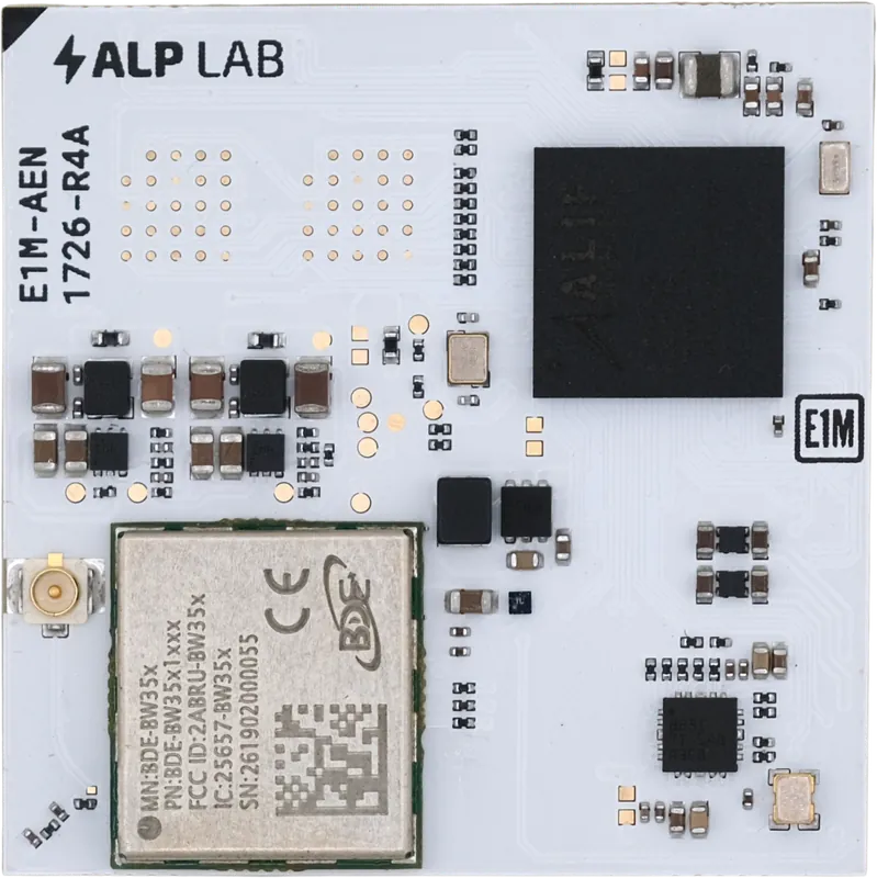
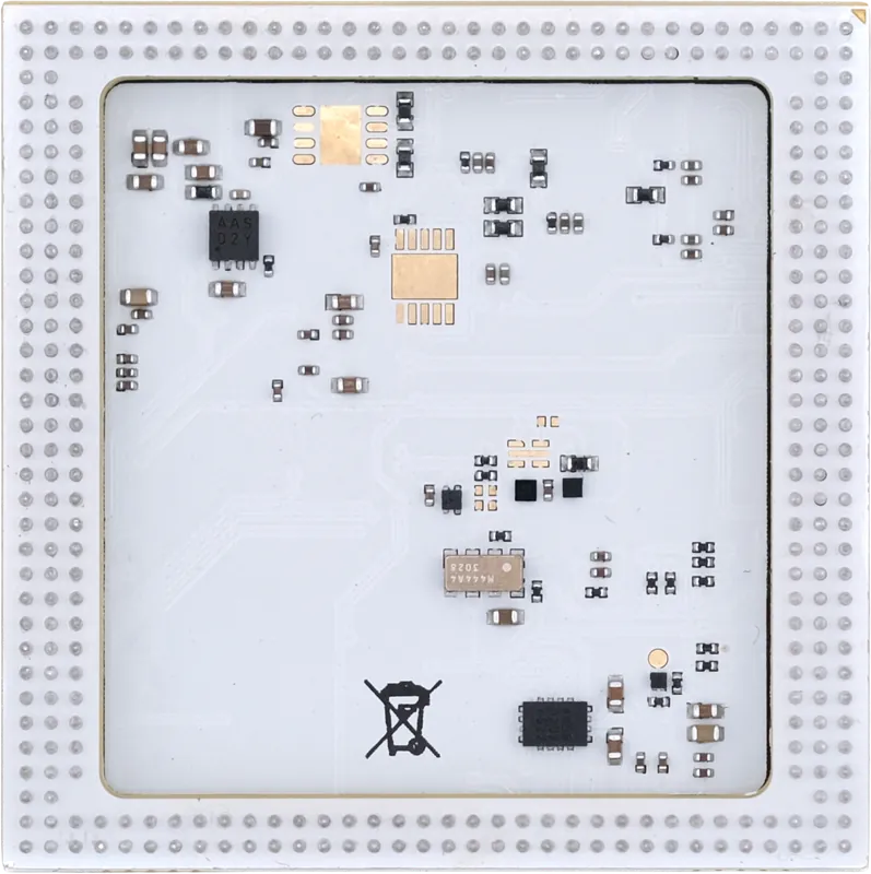
The E1M-AEN Ensemble series modules use the open-source Edge-1 AI Module (E1M™) form factor, with a unified pin layout and hardware functionality. This footprint allows users to interchange MCU/MPU modules seamlessly while keeping hardware compatible. E1M™ is designed for flexibility, functionality, and longevity in high- and medium-range MCU/MPUs.
Features
- Various core options with the same footprint, based on the Alif Semi Ensemble MCU/MPU series:
- E8 — 2 × 800 MHz ARM A32, 2 × ARM M55, 2 × ARM Ethos U55 + 1 × ARM Ethos U85
- E7 — 2 × 800 MHz ARM A32, 2 × ARM M55, 2 × ARM Ethos U55
- E6 — 1 × 800 MHz ARM A32, 2 × ARM M55, 2 × ARM Ethos U55 + 1 × ARM Ethos U85
- E5 — 1 × 800 MHz ARM A32, 2 × ARM M55, 2 × ARM Ethos U55
- E4 — 2 × ARM M55, 2 × ARM Ethos U55 + 1 × ARM Ethos U85
- E3 — 2 × ARM M55, 2 × ARM Ethos U55
- Internal memory: 128 KB – 13.5 MB SRAM on-die, 256 KB – 5.5 MB MRAM
- External memory: up to 2 × OSPI (configurable RAM or ROM)
- MIPI DSI display output, 2 lanes, up to 1.25 Gbps/lane
- MIPI CSI-2 camera input, 2 lanes
- Dual-band (2.4 GHz / 5 GHz) Wi-Fi 6 with up to 20 Mbps throughput
- Bluetooth LE 5.4
- 100 Mbps Ethernet PHY
- CAN-BUS PHY
- Assembly variants available for cost reduction
- Small size: 35 × 35 mm
Applications
IoT, industrial, robotics, motor drive, drones, mobile PoS, smart speakers, object detection, medical devices, vending machines, smart home, process control, smart appliances, scanners.
General Description
Highlights
The Alp Lab E1M-AEN System-on-Module (SoM) is a low-power, cost-effective solution for edge-AI applications. Powered by the Alif Semiconductor Ensemble series processor, it features an Arm Cortex-A32 application CPU (up to 2 × 800 MHz), Arm Cortex-M55 real-time cores, integrated Arm Ethos U55 / U85 NPUs, and an optional JPEG encoder and ISP, making it suitable for low-power edge-AI tasks.
The E1M-AEN supports one camera over a 2-lane MIPI CSI-2 interface and provides customizable options including on-board Wi-Fi / Bluetooth, multiple memory and storage configurations, and PHY variants.
Block Diagram

Module Variants
The E1M-AEN family ships in six MPN variants that share a common E1M™ footprint. Variants differ in the Ensemble SoC used, the application-CPU (A32) count, and the on-die NPU/ISP configuration. See Ordering Information for the full ordering matrix and MPN decoder; the table below summarises the differences.
Table: E1M-AEN Variant Summary
| MPN | Ensemble | A32 cores | NPUs | ISP / JPEG |
|---|---|---|---|---|
| E1M-AEN301 | E3 | — | 2 × U55 | — |
| E1M-AEN501 | E5 | 1 × 800 MHz | 2 × U55 | — |
| E1M-AEN701 | E7 | 2 × 800 MHz | 2 × U55 | — |
| E1M-AEN401 | E4 | — | 2 × U55 + 1 × U85 | Yes |
| E1M-AEN601 | E6 | 1 × 800 MHz | 2 × U55 + 1 × U85 | Yes |
| E1M-AEN801 | E8 | 2 × 800 MHz | 2 × U55 + 1 × U85 | Yes |
Alif Semi Ensemble MCUs/MPUs
This document should be read together with the corresponding Alif Semiconductor Ensemble MCU/MPU datasheet.
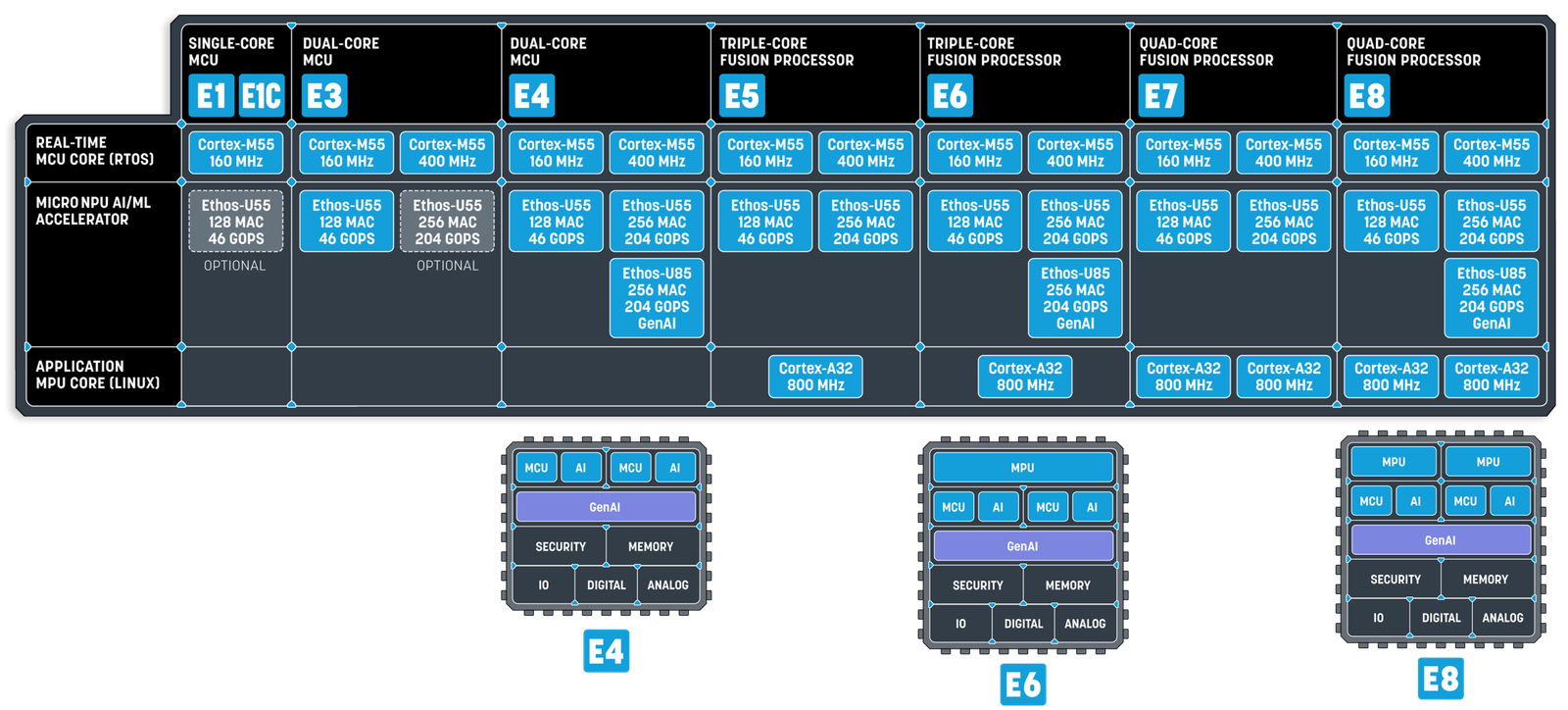
Table: Ensemble MPU Options
| Ensemble | MCU | MPU | NPU | Internal Memory | External Memory | ISP / JPEG |
|---|---|---|---|---|---|---|
| E3 | 2 × M55 | — | 2 × U55 | 5.5 MB – 13.5 MB | 2 × OSPI | — |
| E5 | 2 × M55 | 1 × A32 800 MHz | 2 × U55 | 5.5 MB – 13.5 MB | 2 × OSPI | — |
| E7 | 2 × M55 | 2 × A32 800 MHz | 2 × U55 | 5.5 MB – 13.5 MB | 2 × OSPI | — |
| E4 | 2 × M55 | — | 2 × U55 + 1 × U85 | 5.5 MB – 9.75 MB | 2 × OSPI | Yes |
| E6 | 2 × M55 | 1 × A32 800 MHz | 2 × U55 + 1 × U85 | 5.5 MB – 9.75 MB | 2 × OSPI | Yes |
| E8 | 2 × M55 | 2 × A32 800 MHz | 2 × U55 + 1 × U85 | 5.5 MB – 9.75 MB | 2 × OSPI | Yes |
Pin Diagram and List
The E1M™ standard defines the primary pin functions; the pin-out below follows that standard. Pins can be reassigned to alternate functions in software, but hardware compatibility with other E1M variants will no longer hold because each MCU/MPU has a different pin structure and peripheral mapping.
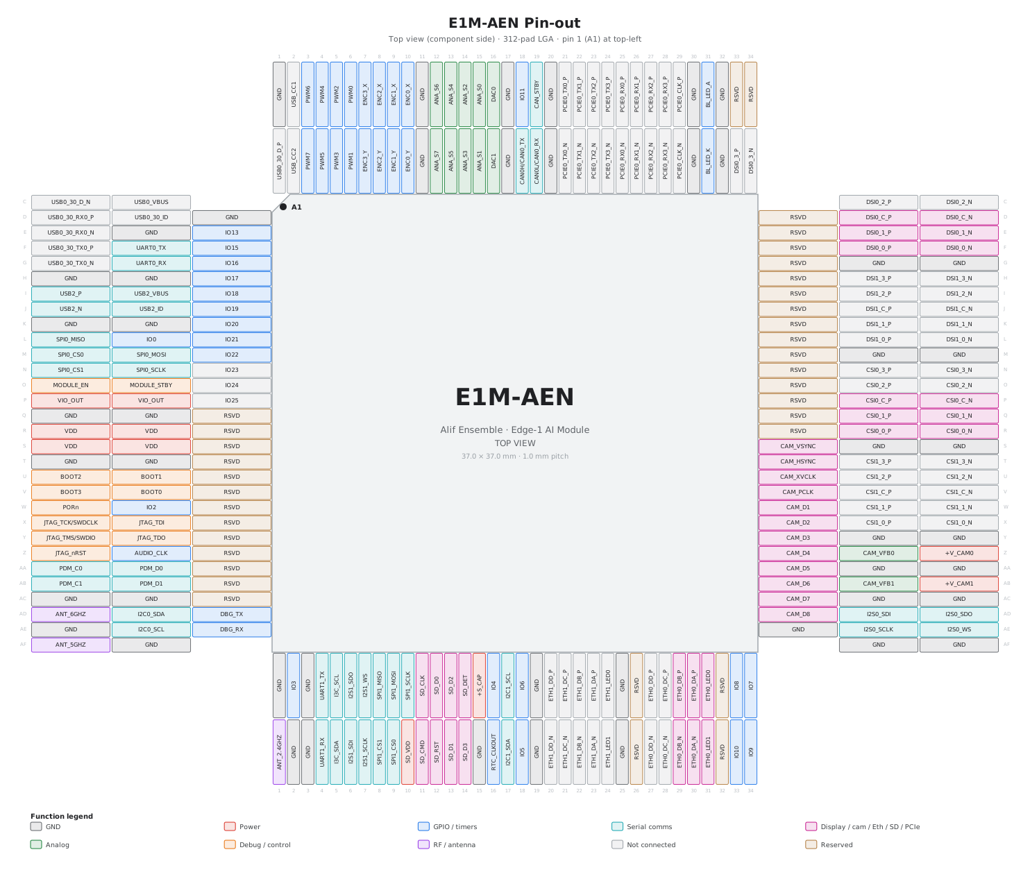
Power & Control Pins
Table: E1M-AEN Power & Control Pins
| Pin Number | Pin Name | Description |
|---|---|---|
| A1, A11, A17, A20, A30, A32, AA33, AA34, AC1, AC2, AC33, AC34, AE1, AE32, AF2, AF33, AF34, AG1, AG3, AG19, AG25, AH2, AH3, AH15, AH19, AH25, B11, B17, B20, B30, B32, D3, E2, G33, G34, H1, H2, K1, K2, M33, M34, Q1, Q2, S33, S34, T1, T2, Y33, Y34 | GND | Ground. |
| R1, S1, R2, S2 | VDD | +5V main supply input to the module. |
| P1, P2 | VIO_OUT | +1V8 output for IO power, up to 200 mA. |
| Z34 | +V_CAM0 | Adjustable LDO output (TLV77201). 0.6 V to 3.3 V, 300 mA max. Camera rail or general-purpose carrier load. |
| AB34 | +V_CAM1 | Adjustable LDO output (TLV77201). 0.6 V to 3.3 V, 300 mA max. Camera rail or general-purpose carrier load. |
| Z33 | CAM_VFB0 | Feedback node for +V_CAM0. Set output voltage via external divider; place close to the module pin. |
| AB33 | CAM_VFB1 | Feedback node for +V_CAM1. Set output voltage via external divider; place close to the module pin. |
| AH10 | SD_VDD | SD/eMMC card power output. |
| AG15 | +S_CAP | Not available for Alif Ensemble series. |
| O1 | MODULE_EN | Module enable. Open-drain. Pulled up internally to VDD. Connect to GND to disable the module; leave floating if not used. |
| O2 | MODULE_STBY | Module stand-by. Pulled up internally to 1V8. On E1M-AEN, stand-by is supported only for the real-time clock. Leave floating if not used. |
| W1 | PORn | Reset input. Open-drain. Pulled up internally to 1V8. Pull low to reset the module; leave floating if not used. |
| U1 | BOOT2 | E1M boot-strap pins. Alif SoCs do not have boot-mode pins; not used on E1M-AEN. Leave floating. |
| U2 | BOOT1 | |
| V1 | BOOT3 | |
| V2 | BOOT0 | |
| X1 | JTAG_TCK/SWDCLK | JTAG/SWD pins for programming and debug. |
| X2 | JTAG_TDI | |
| Y1 | JTAG_TMS/SWDIO | |
| Y2 | JTAG_TDO | |
| Z1 | JTAG_nRST | |
| AH1 | ANT_2.4GHZ | Primary antenna feed (RF_ANT) from the on-module BDE-BW3551N. Route 50 Ω trace to the antenna or connector. |
| AF1 | ANT_5GHZ | Separate 5 GHz feed. The BDE-BW3551N uses a single combined antenna port (ANT_2.4GHZ), so this pin is not used on E1M-AEN. Leave floating. |
| AD1 | ANT_6GHZ | 6 GHz antenna (Wi-Fi 6E). Not used on E1M-AEN. Leave floating. |
| A31 | BL_LED_A | Backlight LED anode / BL_PWM. Connect to backlight driver. |
| B31 | BL_LED_K | Backlight LED cathode. Leave floating if BL_PWM is used. |
Analog Pins
Table: E1M-AEN Analog Pins
| Pin Number | Pin Name | Peripheral | Description |
|---|---|---|---|
| A12 | ANA_S6 | AIN | Analog input channels, referenced to 1V8. |
| A13 | ANA_S4 | ||
| A14 | ANA_S2 | ||
| A15 | ANA_S0 | ||
| B12 | ANA_S7 | ||
| B13 | ANA_S5 | ||
| B14 | ANA_S3 | ||
| B15 | ANA_S1 | ||
| A16 | DAC0 | DAC0 | Analog output channel, referenced to 1V8. |
| B16 | DAC1 | DAC1 | Analog output channel, referenced to 1V8. |
Digital Pins
Table: E1M-AEN Digital Pins
| Pin Number | Pin Name | Peripheral | Description |
|---|---|---|---|
| A18 | IO11 | GPIO | General purpose input/output. |
| AG2 | IO3 | ||
| AG16 | IO4 | ||
| AG18 | IO6 | ||
| AG33 | IO8 | ||
| AG34 | IO7 | ||
| AH18 | IO5 | ||
| AH33 | IO10 | ||
| AH34 | IO9 | ||
| E3 | IO13 | ||
| F3 | IO15 | ||
| G3 | IO16 | ||
| H3 | IO17 | ||
| I3 | IO18 | ||
| J3 | IO19 | ||
| K3 | IO20 | ||
| L2 | IO0 | ||
| W2 | IO2 | ||
| Z2 | AUDIO_CLK | — | Audio clock output. |
| AA1 | PDM_C0 | PDM0 | Digital microphone interface. |
| AA2 | PDM_D0 | ||
| AB1 | PDM_C1 | PDM1 | Digital microphone interface. |
| AB2 | PDM_D1 | ||
| AD33 | I2S0_SDI | I2S0 | I2S interface. |
| AD34 | I2S0_SDO | ||
| AE33 | I2S0_SCLK | ||
| AE34 | I2S0_WS | ||
| AG6 | I2S1_SDO | I2S1 | I2S interface. |
| AG7 | I2S1_WS | ||
| AH6 | I2S1_SDI | ||
| AH7 | I2S1_SCLK | ||
| AD2 | I2C0_SDA | I2C0 | I2C interface. |
| AE2 | I2C0_SCL | ||
| AG17 | I2C1_SCL | I2C1 | I2C interface. |
| AH17 | I2C1_SDA | ||
| AG5 | I3C_SCL | I3C | I3C interface. |
| AH5 | I3C_SDA | ||
| L1 | SPI0_MISO | SPI0 | SPI interface. |
| M1 | SPI0_CS0 | ||
| M2 | SPI0_MOSI | ||
| N1 | SPI0_CS1 | ||
| N2 | SPI0_SCLK | ||
| AG8 | SPI1_MISO | SPI1 | SPI interface. |
| AG9 | SPI1_MOSI | ||
| AG10 | SPI1_SCLK | ||
| AH8 | SPI1_CS1 | ||
| AH9 | SPI1_CS0 | ||
| F2 | UART0_TX | UART0 | UART interface. |
| G2 | UART0_RX | ||
| AG4 | UART1_TX | UART1 | UART interface. |
| AH4 | UART1_RX | ||
| A19 | CAN_STBY | CAN0 | CAN-BUS interface. |
| B18 | CAN0H/CAN0_TX | ||
| B19 | CAN0L/CAN0_RX | ||
| A3 | PWM6 | PWM | PWM output. |
| A4 | PWM4 | ||
| A5 | PWM2 | ||
| A6 | PWM0 | ||
| B3 | PWM7 | ||
| B4 | PWM5 | ||
| B5 | PWM3 | ||
| B6 | PWM1 | ||
| A10 | ENC0_X | ENC0 | Encoder input. |
| B10 | ENC0_Y | ||
| A9 | ENC1_X | ENC1 | Encoder input. |
| B9 | ENC1_Y | ||
| A8 | ENC2_X | ENC2 | Encoder input. |
| B8 | ENC2_Y | ||
| A7 | ENC3_X | ENC3 | Encoder input. |
| B7 | ENC3_Y | ||
| AG29 | ETH0_DB_P | ETH0 | Ethernet interface. 100 Mbit PHY connection. |
| AG30 | ETH0_DA_P | ||
| AG31 | ETH0_LED0 | ||
| AH29 | ETH0_DB_N | ||
| AH30 | ETH0_DA_N | ||
| AH31 | ETH0_LED1 | ||
| AG11 | SD_CLK | SD0 | SD card or eMMC interface. |
| AG12 | SD_D0 | ||
| AG13 | SD_D2 | ||
| AG14 | SD_DET | ||
| AH11 | SD_CMD | ||
| AH12 | SD_RST | ||
| AH13 | SD_D1 | ||
| AH14 | SD_D3 | ||
| P33 | CSI0_C_P | CSI0 | MIPI CSI-2 camera interface. |
| P34 | CSI0_C_N | ||
| Q33 | CSI0_1_P | ||
| Q34 | CSI0_1_N | ||
| R33 | CSI0_0_P | ||
| R34 | CSI0_0_N | ||
| D33 | DSI0_C_P | DSI0 | MIPI DSI display interface. |
| D34 | DSI0_C_N | ||
| E33 | DSI0_1_P | ||
| E34 | DSI0_1_N | ||
| F33 | DSI0_0_P | ||
| F34 | DSI0_0_N | ||
| AA32 | CAM_D5 | CAM_PAR | Parallel camera interface. |
| AB32 | CAM_D6 | ||
| AC32 | CAM_D7 | ||
| AD32 | CAM_D8 | ||
| S32 | CAM_VSYNC | ||
| T32 | CAM_HSYNC | ||
| U32 | CAM_XVCLK | ||
| V32 | CAM_PCLK | ||
| W32 | CAM_D1 | ||
| X32 | CAM_D2 | ||
| Y32 | CAM_D3 | ||
| Z32 | CAM_D4 | ||
| I1 | USB2_P | USB0 | USB 2.0 interface (routed to the E1M standard USB2 pins). |
| J1 | USB2_N | ||
| I2 | USB2_VBUS | ||
| J2 | USB2_ID | ||
| AH16 | RTC_CLKOUT | — | Real-time clock output. |
| AD3 | DBG_TX | DBG | On-module debug UART. Defaults to debug UART; selectable to GPIO. |
| AE3 | DBG_RX |
Not Connected Pins
These pins carry an E1M standard function that is not implemented on E1M-AEN. They retain their standard name for cross-variant compatibility and must be left floating.
Table: E1M-AEN Not-connected Pins
| Pin Number | Pin Name | Description |
|---|---|---|
| AG27 | ETH0_DD_P | ETH0 gigabit pairs (DC/DD) — E1M-AEN Ethernet is 100 Mbit. Leave floating. |
| AG28 | ETH0_DC_P | |
| AH27 | ETH0_DD_N | |
| AH28 | ETH0_DC_N | |
| AG20 | ETH1_DD_P | Second Ethernet (ETH1) — not implemented on E1M-AEN. Leave floating. |
| AG21 | ETH1_DC_P | |
| AG22 | ETH1_DB_P | |
| AG23 | ETH1_DA_P | |
| AG24 | ETH1_LED0 | |
| AH20 | ETH1_DD_N | |
| AH21 | ETH1_DC_N | |
| AH22 | ETH1_DB_N | |
| AH23 | ETH1_DA_N | |
| AH24 | ETH1_LED1 | |
| A21 | PCIE0_TX0_P | PCI Express (PCIE0) — not implemented on E1M-AEN. Leave floating. |
| A22 | PCIE0_TX1_P | |
| A23 | PCIE0_TX2_P | |
| A24 | PCIE0_TX3_P | |
| A25 | PCIE0_RX0_P | |
| A26 | PCIE0_RX1_P | |
| A27 | PCIE0_RX2_P | |
| A28 | PCIE0_RX3_P | |
| A29 | PCIE0_CLK_P | |
| B21 | PCIE0_TX0_N | |
| B22 | PCIE0_TX1_N | |
| B23 | PCIE0_TX2_N | |
| B24 | PCIE0_TX3_N | |
| B25 | PCIE0_RX0_N | |
| B26 | PCIE0_RX1_N | |
| B27 | PCIE0_RX2_N | |
| B28 | PCIE0_RX3_N | |
| B29 | PCIE0_CLK_N | |
| B1 | USB0_30_D_P | USB0 port — not used on E1M-AEN; the USB 2.0 interface is routed to the USB2 pins. Leave floating. |
| C1 | USB0_30_D_N | |
| C2 | USB0_VBUS | |
| D2 | USB0_30_ID | |
| A2 | USB_CC1 | USB SuperSpeed lanes and USB-C configuration — not used on E1M-AEN. Leave floating. |
| B2 | USB_CC2 | |
| D1 | USB0_30_RX0_P | |
| E1 | USB0_30_RX0_N | |
| F1 | USB0_30_TX0_P | |
| G1 | USB0_30_TX0_N | |
| B33 | DSI0_3_P | MIPI DSI0 lanes 2 and 3 — E1M-AEN DSI is 2-lane. Leave floating. |
| B34 | DSI0_3_N | |
| C33 | DSI0_2_P | |
| C34 | DSI0_2_N | |
| H33 | DSI1_3_P | Second MIPI DSI (DSI1) — not implemented on E1M-AEN. Leave floating. |
| H34 | DSI1_3_N | |
| I33 | DSI1_2_P | |
| I34 | DSI1_2_N | |
| J33 | DSI1_C_P | |
| J34 | DSI1_C_N | |
| K33 | DSI1_1_P | |
| K34 | DSI1_1_N | |
| L33 | DSI1_0_P | |
| L34 | DSI1_0_N | |
| N33 | CSI0_3_P | MIPI CSI0 lanes 2 and 3 — E1M-AEN CSI is 2-lane. Leave floating. |
| N34 | CSI0_3_N | |
| O33 | CSI0_2_P | |
| O34 | CSI0_2_N | |
| T33 | CSI1_3_P | Second MIPI CSI (CSI1) — not implemented on E1M-AEN. Leave floating. |
| T34 | CSI1_3_N | |
| U33 | CSI1_2_P | |
| U34 | CSI1_2_N | |
| V33 | CSI1_C_P | |
| V34 | CSI1_C_N | |
| W33 | CSI1_1_P | |
| W34 | CSI1_1_N | |
| X33 | CSI1_0_P | |
| X34 | CSI1_0_N | |
| L3 | IO21 | GPIO not bonded on E1M-AEN. Leave floating. |
| M3 | IO22 | |
| N3 | IO23 | |
| O3 | IO24 | |
| P3 | IO25 |
Reserved Pins
Table: E1M-AEN Reserved Pins
| Pin Number | Pin Name | Description |
|---|---|---|
| A33, A34, AA3, AB3, AC3, AG26, AG32, AH26, AH32, D32, E32, F32, G32, H32, I32, J32, K32, L32, M32, N32, O32, P32, Q3, Q32, R3, R32, S3, T3, U3, V3, W3, X3, Y3, Z3 | RSVD | Do not connect. Used for production purposes. |
Specifications
Absolute Maximum Ratings
Warning: Stresses beyond Absolute Maximum Ratings may cause permanent damage. Operation at these conditions is not implied.
Table: E1M-AEN Absolute Maximum Ratings
| Parameter | Symbol | Min | Max | Unit |
|---|---|---|---|---|
| Power-supply voltage | VDDIN to GND | − 0.3 | 6.0 | V |
| Analog input voltage | V(ANA_Sx) | − 0.3 | 1.98 | V |
| Digital IO (1V8) | − 0.3 | 1.98 | V | |
| CAN bus voltage (CAN0H / CAN0L) | V(CANx) | − 58 | +58 | V |
| Ethernet MDI (TD±, RD±) | V(MDI) | − 0.3 | +4 | V |
| Backlight boost switch node | V(LX) | − 0.3 | +40 | V |
| Maximum junction temperature | TJ | − 40 | +150 | °C |
Recommended Operating Conditions
The module is specified to meet the Electrical Characteristics in Electrical Characteristics over the conditions below. Operation outside this range is not guaranteed.
Table: E1M-AEN Recommended Operating Conditions
| Parameter | Symbol | Min | Typ | Max | Unit |
|---|---|---|---|---|---|
| Module supply voltage | VDDIN | 4.5 | 5.0 | 5.5 | V |
| Ambient operating temperature | TA | − 40 | — | +85 | °C |
| Relative humidity (operating, non-condensing) | RH | TBD | — | TBD | % |
Electrical Characteristics
Table: E1M-AEN Electrical Characteristics
| Symbol | Description | Min | Nom | Max | Unit |
|---|---|---|---|---|---|
| Power supply | |||||
| IDDMAX | Maximum IDD current | — | — | TBD | mA |
| Analog inputs | |||||
| V(AINx) | Input voltage | 0 | — | 1.8 | V |
| Digital IOs (1.8 V LVCMOS) | |||||
| VOL | Low-level output voltage (at rated IOL) | — | — | 0.4 | V |
| VOH | High-level output voltage (at rated IOH) | 1.4 | — | — | V |
| VIL | Low-level input voltage | — | — | 0.63 | V |
| VIH | High-level input voltage | 1.17 | — | — | V |
| Adjustable LDO outputs (+V_CAM0 / +V_CAM1) | |||||
| +V_CAM0 | Adjustable LDO output (TLV77201) | 0.6 | — | 3.3 | V |
| +V_CAM1 | Adjustable LDO output (TLV77201) | 0.6 | — | 3.3 | V |
Note: Digital IO levels assume 1.8 V LVCMOS signalling (VIL ≤ 0.35·VDDIO, VIH ≥ 0.65·VDDIO). Confirm against the final Alif Ensemble SoC datasheet revision for the configured drive strength.
ESD & Latch-up Ratings
ESD ratings apply at module-level — i.e. directly to the LGA pads as exposed to a carrier-board assembly process. The values below reflect the Ensemble SoC silicon ratings as seen at the LGA pads. With the exception of the SDIO / SD-card interface — which retains on-module ESD protection and series resistors — the module does not integrate interface ESD or EMI protection; the carrier board must provide external ESD/EMI protection on all exposed external-facing interfaces, as described in the relevant interface sub-sections. The HFXO / LFXO clock pins are not exposed on the module.
Table: E1M-AEN ESD & Latch-up Ratings
| Parameter | Standard | Min | Max | Unit |
|---|---|---|---|---|
| Human Body Model (HBM) | ANSI/ESDA/JEDEC JS-001 | ± 2000 | — | V |
| Charged Device Model (CDM) | ANSI/ESDA/JEDEC JS-002 | ± 250 | — | V |
| Latch-up | JESD78 | ± 100 | — | mA |
Thermal Characteristics
The E1M-AEN dissipates heat primarily through the Ensemble SoC. The thermal-resistance figures below are the Ensemble SoC package values (FBGA194, junction-to-free-air in natural convection per the Alif datasheet); the realised module-level performance additionally depends on carrier-board copper area, airflow, and via stitching. Maximum junction temperature is the Ensemble SoC operating limit (absolute maximum +150 °C, see Absolute Maximum Ratings).
Table: E1M-AEN Thermal Characteristics
| Parameter | Symbol | Typ | Max | Unit |
|---|---|---|---|---|
| Thermal resistance, junction-to-ambient (still air) | θJA | 21.1 | — | °C/W |
| Thermal resistance, junction-to-case | θJC | 17.0 | — | °C/W |
| Maximum junction temperature | TJ,max | — | +105 | °C |
| Power dissipation derating (above +85 °C) | PD | TBD | — | mW/°C |
Power-dissipation derating curve (figure pending)
Power
Power Architecture
All power rails on the module are generated and managed on-board from a single externally-supplied 5 V input on the VDDIN pads. On-module power management is performed by an integrated PMIC, which brings up and sequences all internal rails automatically; the carrier board supplies a single 5 V input and does not need to sequence any power rails.
The E1M-AEN includes all necessary decoupling capacitors. Additional decoupling capacitors on the carrier board may improve performance further.
The module exposes the following regulated output rails to the carrier:
Table: Module Output Rails
| Rail | Pins | Voltage | Max current | Purpose |
|---|---|---|---|---|
| VIO_OUT | P1, P2 | 1.8 V ± 5% | 200 mA | I/O reference for carrier-side level shifters. |
| +V_CAM0 | Z34 | 0.6 – 3.3 V (adj.) | 300 mA | Adjustable LDO (TLV77201), set via CAM_VFB0. Camera rail or general-purpose carrier load. |
| +V_CAM1 | AB34 | 0.6 – 3.3 V (adj.) | 300 mA | Adjustable LDO (TLV77201), set via CAM_VFB1. Camera rail or general-purpose carrier load. |
E1M-AEN Power Architecture Diagram (figure pending)
Power-Up & Reset Sequence
No power-rail sequencing is required — the on-module PMIC handles rail bring-up. The steps below are the recommended carrier-side control-signal bring-up order:
- Apply 5 V to
VDDIN. - Release
MODULE_EN(let internal pull-up hold high). - Release
PORn(let internal pull-up hold high). - Wait for the internal rails to stabilise and the SoC boot ROM to start. Power-up time is TBD ms.
- Begin communication with the module.

Note: For power-down, drive
MODULE_ENlow and removeVDDIN. The module does not require a controlled power-down sequence at the carrier-board level.
Power Consumption
Numbers below are typical at TA = +25 °C, VDDIN = 5.0 V, with Wi-Fi and BLE disabled unless otherwise noted. Active and low-power figures depend on the Ensemble variant and software workload.
Table: E1M-AEN Power Consumption (typical)
| Mode | Description | Min | Typ | Max | Unit |
|---|---|---|---|---|---|
| Active | |||||
| Active, A32 + M55 + NPU @ full clock | Worst-case AI inference | — | TBD | TBD | mA |
| Active, A32 idle / M55 running | Real-time only | — | TBD | TBD | mA |
| Active, with Wi-Fi 6 TX @ +20 dBm | Wireless TX peak | — | TBD | TBD | mA |
| Low-power | |||||
| Idle | Cores halted, peripherals on | — | TBD | — | mA |
| Sleep | Retention only, RTC running | — | TBD | — | μA |
| Shutdown (MODULE_EN low) | Module disabled | — | TBD | — | μA |
Boot Modes
Alif Semiconductor SoCs have no boot-mode strap pins; the boot flow is fixed and programmed into the internal ROM. The E1M BOOT0–BOOT3 strap pins defined in the E1M™ specification are therefore not used on E1M-AEN and should be left floating.
The boot ROM loads the application image from MRAM. External boot sources (OSPI flash, SD card) are selected in software once the boot ROM is running.
Note: Refer to the Alif Semiconductor Ensemble series boot reference manual for the internal boot sequence and image-signing requirements.
Reset & Module Enable
The E1M-AEN exposes three carrier-controllable control signals:
Table: Reset & Module Enable Signals
| Pin | Direction | Description |
|---|---|---|
MODULE_EN | Input, open-drain | Internally pulled up to VDDIN. Pull low to disable the module (forces shutdown). Leave floating if unused. |
PORn | Input, open-drain | Internally pulled up to 1V8. Pull low to issue a power-on reset to the SoC. Minimum low-pulse width: TBD μs. |
MODULE_STBY | Input, open-drain | Internally pulled up to 1V8. On E1M-AEN, stand-by is supported only for the real-time clock. Leave floating if unused. |

JTAG / SWD Debug
The E1M-AEN exposes a 5-pin JTAG/SWD interface for programming and debug. Signals operate at 1.8 V; carrier-board level shifters are required for 3.3 V debug probes.
Table: JTAG / SWD Pinout
| Pin | Signal | Description |
|---|---|---|
| Z1 | JTAG_nRST | Active-low reset to the SoC debug logic. |
| X1 | JTAG_TCK / SWDCLK | Test clock (JTAG) or serial-wire clock (SWD). |
| X2 | JTAG_TDI | Test data in (JTAG only). |
| Y2 | JTAG_TDO | Test data out (JTAG only). |
| Y1 | JTAG_TMS / SWDIO | Test mode select (JTAG) or serial-wire I/O (SWD). |
Note: Alp Lab recommends exposing the JTAG/SWD pins on a 10-pin Cortex-M debug header on the carrier board. Refer to the E1M Hardware Design Guide for the reference connector pinout.
Reference JTAG / SWD Header Pinout (figure pending)
Interfaces
Ethernet
E1M-AEN has one 100 Mbit Ethernet PHY: the TI DP83825I. The interface does not include on-module EMI or ESD protection; the user must provide an external magnetics transformer, connector, and EMI/ESD protection on the carrier board.

The PHY is configured as follows:
Table: Ethernet PHY Configuration
| Function | Setting | Description |
|---|---|---|
| Auto-Negotiation | Enabled | Auto-Negotiation is enabled by default. |
| Auto MDI/MDIX | Enabled | Auto-MDIX is enabled by default. |
Note: The DP83825I MDI pins (TD±, RD±) integrate ± 5 kV IEC 61000-4-2 ESD protection. External magnetics, connector, and additional EMI/ESD protection are still required on the carrier board.
USB
E1M-AEN has one USB 2.0 interface. It supports Full-Speed (12 Mbit/s) and High-Speed (480 Mbit/s) bit rates and can operate as device or host.
Table: E1M-AEN USB Interface
| Pin Number | Pin Name | Peripheral | Description |
|---|---|---|---|
| I1 | USB2_P | USB0 | Route USB2_P and USB2_N as a differential pair with 90 Ω impedance. |
| J1 | USB2_N | ||
| J2 | USB2_ID | Low: Host mode. NC: Device mode. | |
| I2 | USB2_VBUS | Connect to USB VBUS 5 V. |
Note: The USB 2.0 interface is brought out on the E1M standard
USB2pins (I1/J1). TheUSB0pins (B1/C1/...), which carry the standard's optional USB 3.x SuperSpeed lanes, are not used on E1M-AEN and must be left floating.
Serial Interfaces
I2C
E1M-AEN exposes two I²C interfaces. Refer to the Alif Semiconductor Ensemble series datasheet for full details. External pull-ups are required.
I3C
E1M-AEN exposes one I³C interface. Refer to the Alif Semiconductor Ensemble series datasheet for full details. External pull-ups are required.
UART
E1M-AEN exposes two UART interfaces. Refer to the Alif Semiconductor Ensemble series datasheet for full details.
Note: One UART interface is connected to the secondary MCU on E1M. It is handled by the Alp SDK™ from the main MPU.
SPI
E1M-AEN exposes two SPI interfaces. Refer to the Alif Semiconductor Ensemble series datasheet for full details.
Note: One SPI interface is connected to the secondary MCU on E1M. It is handled by the Alp SDK™ from the main MPU.
I2S
E1M-AEN exposes two I²S interfaces. Refer to the Alif Semiconductor Ensemble series datasheet for full details.
CAN Bus
E1M-AEN includes an optional CAN-BUS PHY (TI TCAN1044AVDRBRQ1) to simplify carrier-board hardware design. When the internal PHY is used, the user must add termination, ESD, and EMI protection components on the carrier board.

Note: The TCAN1044AVDRBRQ1 bus pins withstand ± 8 kV unpowered contact discharge and ± 15 kV air discharge per ISO 10605.
Wireless Module & Antenna
E1M-AEN includes an on-board BDE-BW3551N dual-band (2.4 GHz / 5 GHz) Wi-Fi 6 and Bluetooth LE 5.4 combo module, based on the Texas Instruments SimpleLink™ CC3551E wireless MCU SoC. The module is backward-compatible with Wi-Fi 4 (802.11 a/b/g/n) and Wi-Fi 5 (802.11 ac). Its single-stream radio supports 20 MHz channels with application throughput up to 20 Mbps (UDP), and WPA / WPA2 / WPA3 personal and enterprise security. The module ANT output is brought out to the ANT pad (AH1) and may be routed to a U.FL connector or a carrier-board PCB antenna. Antenna selection is optional.

RF Characteristics
Table: E1M-AEN Wi-Fi 6 / BLE RF Characteristics
| Symbol | Description | Min | Typ | Max | Unit |
|---|---|---|---|---|---|
| Wi-Fi 6 (802.11ax, 2.4 GHz) | |||||
| fop | Operating frequency range | 2412 | — | 2472 | MHz |
| PTX | TX output power (HE MCS0) | — | 18.2 | — | dBm |
| PTX | TX output power (HE MCS7) | — | 15.7 | — | dBm |
| PRX | RX sensitivity (HE MCS0, 4K) | — | −89 | — | dBm |
| PRX | RX sensitivity (HE MCS7, 4K) | — | −70 | — | dBm |
| Wi-Fi 6 (802.11ax, 5 GHz) | |||||
| fop | Operating frequency range | 5180 | — | 5845 | MHz |
| PTX | TX output power (HE MCS0) | — | 19.7 | — | dBm |
| PTX | TX output power (HE MCS7) | — | 14.1 | — | dBm |
| PRX | RX sensitivity (HE MCS0, 4K) | — | −91.5 | — | dBm |
| PRX | RX sensitivity (HE MCS7, 4K) | — | −71.5 | — | dBm |
| η | Max application throughput (UDP) | — | 20 | — | Mbps |
| Bluetooth LE 5.4 | |||||
| fop | Operating frequency range | 2402 | — | 2480 | MHz |
| PTX | TX output power (max setting) | — | 16.3 | — | dBm |
| PRX | RX sensitivity (LE 1M, 37-byte) | — | −97.5 | — | dBm |
| PRX | RX sensitivity (LE Coded, 125 kbps) | — | −103.5 | — | dBm |
Note: Radio figures are BDE-BW3551N module specifications (typical, averaged across all channels). Values at the carrier-board antenna will be reduced by trace and connector losses.
Antenna Options
The E1M-AEN antenna port can be routed three ways:
- On-module U.FL connector — connect an external antenna directly to the module.
- Carrier-board PCB antenna — route the
ANTpad (AH1) out as a 50 Ω controlled-impedance trace to a chip or PCB antenna on the carrier board. - Carrier-board RF connector — extend the 50 Ω trace to a U.FL / IPEX / SMA connector on the carrier board.
Maximum antenna gain to maintain regulatory compliance is TBD dBi.
Regulatory Information
The on-module Wi-Fi 6 / BLE 5.4 combo is pre-certified for the regions listed below. Reusing the module's certifications on the customer's end product requires following the integration guidelines in the relevant certification reports.
Table: Wireless Regulatory Approvals
| Region | Standard | Certificate ID | Notes |
|---|---|---|---|
| United States | FCC Part 15 | TBD | Modular grant pending. |
| Europe | RED / CE | TBD | — |
| Canada | ISED RSS-247 | TBD | — |
| Japan | MIC (Japan) | TBD | — |
Note: The on-module BDE-BW3551N wireless module is rated for ± 4 kV contact-discharge and ± 8 kV air-discharge ESD per EN 301-489. This is a module-level figure for the wireless subsystem; E1M-AEN pad-level HBM/CDM ratings are listed in the ESD & Latch-up Ratings table.
Warning: Certifications apply only when the module is used with the antenna(s) listed in the certification report. Using an unlisted antenna voids the modular grant and requires re-certification on the customer's end product.
SD Card
E1M-AEN supports an external μSD card over the SDIO interface. The SDIO lines are protected on the module by an NXP NVT4858HKZ, which integrates an EMI filter and ESD protection, plus 33 Ω series resistors.

Note: The NVT4858HKZ provides IEC 61000-4-2 level 4 ESD protection: ± 8 kV contact discharge and ± 15 kV air discharge.
MIPI DSI Display & Backlight Controller
The Alif Ensemble series exposes a 2-lane MIPI DSI interface (D-PHY Tx, MIPI DSI v1.2 / D-PHY v1.2) for an external display: up to 1.25 Gbps per lane (2.5 Gbps aggregate), video mode only. The maximum panel resolution and frame rate are limited by the pixel clock and the available DSI link bandwidth (2 lanes × 1.25 Gbps); the Alif E8 datasheet v1.0 (§3.20.2) does not specify a fixed maximum display resolution. The Ensemble series also includes a 2D GPU (D/AVE) that can accelerate display rendering.

The MIPI display and camera interfaces exposed on the module are summarised below.
Table: E1M-AEN MIPI Interface Summary
| Interface | Lanes | Rate / lane | Aggregate | Max resolution |
|---|---|---|---|---|
| MIPI DSI (display, D-PHY Tx) | 2 | 1.25 Gbps | 2.5 Gbps | bandwidth-limited† |
| MIPI CSI-2 (camera, D-PHY Rx) | 2 | 2.5 Gbps | 5.0 Gbps | up to 2 MP (1920 × 1080) |
Note: † The Alif E8 datasheet v1.0 (§3.20.2) specifies no fixed maximum DSI display resolution; the panel ceiling is set by the pixel clock and the 2-lane × 1.25 Gbps D-PHY Tx link bandwidth (video mode only). The 1920 × 1080 (2 MP) figure is the ISP / camera-input ceiling, not a DSI display limit. Both interfaces conform to MIPI D-PHY v1.2. The CSI-2 host supports up to 16 interleaved virtual channels; the DSI supports bidirectional / escape mode on data lane 0. Neither interface includes on-module EMI or ESD protection — protect the lanes with a low-capacitance TVS array on the carrier board.
E1M-AEN has a backlight driver (Kinetic KTD2801ECD-TR) for external screens, controlled directly from the Alp SDK™. The driver is optional; outputs are configured via the BL_LED_A and BL_LED_K pins. The driver supports up to 10 LEDs in series, or 2P6S, and integrates a 36 V over-voltage-protection (OVP) threshold on its boost switch node.
If the backlight driver is not needed, the BL_PWM signal can be exposed directly to drive an external backlight driver. The MIPI DSI interface does not include on-module EMI or ESD protection; protect the DSI lanes with a low-capacitance TVS array on the carrier board.
The feedback resistor value can be computed from the required LED current:
I_LED = 95 mV / R_FB
MIPI CSI Camera
The Alif Ensemble series has a 2-lane MIPI CSI-2 interface (D-PHY Rx, MIPI CSI-2 v1.2 / D-PHY v1.2) for an external camera: up to 2.5 Gbps per lane (5.0 Gbps aggregate), up to 16 interleaved virtual channels, and input resolution up to 2 MP (1920 × 1080). On the E4, E6, and E8 variants the Ensemble SoC also integrates an on-die ISP and JPEG encoder for accelerated image processing (see On-die ISP & JPEG Encoder (E4 / E6 / E8)); the E3, E5, and E7 variants do not.

On-die ISP & JPEG Encoder (E4 / E6 / E8)
On the E4, E6, and E8 variants the Ensemble SoC integrates an Image Signal Processor (ISP) in the data path between the camera interfaces (MIPI CSI / parallel CPI) and memory, plus a JPEG encoder for still-image and Motion-JPEG capture. Both blocks are clocked at up to 400 MHz. The E3, E5, and E7 variants omit both.
The ISP processes up to 2 MP (1920 × 1080) at up to 200 FPS (2 MP image, 100 MHz pixel clock), down to a 64 × 64 minimum output, and offers:
- Input formats: 8-, 10-, 12-bit Bayer; 8-, 10-bit YUV (BT.601 / BT.656); 8-, 10-bit monochrome
- Black-level subtraction, digital gain, demosaicing (Bayer → RGB), and gamma correction
- Colour-space conversion (RGB → YUV), YUV422 → YUV444 → RGB
- Crop / Region-of-Interest, binning, and down-scaling
- Frame-rate control (configurable 60 FPS – 1 FPS)
- Auto-exposure (AE) and auto-white-balance (AWB)
The JPEG encoder compresses up to 2 MP at 200 FPS (32 × 32 minimum, 16K maximum frame width) and offers:
- JPEG ISO/IEC 10918-1 / ITU-T T.81 baseline (Huffman, interleaved YUV420)
- Motion-JPEG (T.81 Annex H) in an AVI container
- Encoding colour space YUV 4:0:0 / 4:2:0 / 4:2:2, 8-bit depth
- Rate control (target bits per picture), slice-mode encoding, 4:2:2 → 4:2:0 conversion, and multi-region alpha blending
Note: These are Ensemble SoC hardware capabilities. ISP/JPEG offload is not yet exposed through the Alp SDK™; see AN-003: MIPI CSI Camera for the current software-enablement status before selecting a variant for its ISP.
E1M supports direct camera implementation via on-board LDOs. Place the feedback resistors as close as possible to the CAM_VFBx pins. The MIPI CSI interface does not include on-module EMI or ESD protection; protect the CSI lanes with a low-capacitance TVS array on the carrier board.
The output voltage is set by the divider:
V_CAM = 0.6 V × (1 + R1 / R2)
To minimize feedback-pin current error, set the divider current to 100 × the maximum feedback-pin current. The resulting series resistance limit is:
R1 + R2 ≤ V_OUT / (I_FB × 100)
where I_FB,nom = 10 nA and I_FB,max = 100 nA.
Parallel Camera
E1M-AEN provides an 8-bit parallel camera interface (CAM_PAR) for sensors that do not use MIPI CSI-2. The interface comprises the 8 data lines CAM_D1–CAM_D8, pixel clock CAM_PCLK, horizontal and vertical sync CAM_HSYNC / CAM_VSYNC, and the sensor master-clock output CAM_XVCLK. Sensor power can be supplied from the on-module adjustable LDO outputs (+V_CAM0 / +V_CAM1).
Microphone – PDM
E1M supports up to 4 digital microphones over 2 PDM interfaces.

Refer to the E1M hardware design guide for full details.
Analog Inputs
E1M provides 8 analog input channels. The Alif Ensemble series has a 12-bit ADC with a 5 Msps sampling rate. Analog inputs are referenced to 1V8.
An optional 0.1% standalone 1V8 reference is available on E1M.
Refer to the Alif Ensemble series datasheet for electrical characteristics.
Analog Outputs
E1M provides 2 analog output channels. The Alif Ensemble series has a 12-bit DAC with a 1 kHz sampling rate. Analog outputs are referenced to 1V8.
Refer to the Alif Ensemble series datasheet for electrical characteristics.
Memories
E1M-AEN offers several memory options. The Alif Ensemble series has internal ROM and RAM of up to 5.5 MB and 13.5 MB respectively.
Two optional OSPI memories are available on E1M-AEN; each can be configured as either RAM or ROM. A single OSPI interface is multiplexed across both memories. External memories are useful when running Linux or when additional RAM is required.
An optional I²C EEPROM is also available, connected through I²C0 on E1M. It can be flashed in production. I²C0 is also accessible on the E1M pinout. Refer to the E1M hardware design guide for details.

Environmental & Reliability
Operating & Storage Conditions
Table: Environmental Conditions
| Parameter | Symbol | Min | Max | Unit |
|---|---|---|---|---|
| Ambient operating temperature | TA | − 40 | +85 | °C |
| Storage temperature | TSTG | − 40 | +125 | °C |
| Relative humidity (operating, non-condensing) | RH | TBD | TBD | % |
Reflow Profile
The E1M-AEN is qualified per IPC/JEDEC J-STD-020 to MSL TBD. The recommended lead-free reflow profile is shown in Reflow Profile, measured on a JTR1000 convection reflow oven using ALPHA OM338 (SAC, Pb-free) solder paste. Peak package temperature is 241–244 °C. Customers must follow the reflow profile below and the dry-pack handling instructions in MSL & Handling.

Table: Reflow Profile Parameters (Pb-free)
| Parameter | Symbol | Min | Max | Unit |
|---|---|---|---|---|
| Average ramp-up rate (TL to TP) | — | — | 3 | °C/s |
| Preheat / soak time (150–217 °C) | tS | 60 | 120 | s |
| Time above liquidus (≥217 °C) | tL | 45 | 90 | s |
| Peak package temperature | TP | 241 | 244 | °C |
| Average ramp-down rate (TP to TL) | — | − 1.6 | — | °C/s |
| Time 25 °C to peak | — | — | 8 | min |
Reliability Data
Table: Reliability Targets
| Parameter | Symbol | Value | Unit |
|---|---|---|---|
| Mean Time Between Failures (Telcordia SR-332, TA = +25 °C) | MTBF | TBD | h |
| Moisture Sensitivity Level | MSL | TBD | — |
| Qualified shelf life (in dry-pack) | — | TBD | months |
Software & Operating System Support
The E1M-AEN is supported by the open-source Alp SDK™, which provides a unified HAL across all E1M variants. Out of the box, the SDK supports:
- Bare-metal application development on the Cortex-M55 real-time cores.
- Zephyr RTOS on the Cortex-M55 cores (BSP
e1m-aenupstream). - Linux on the Cortex-A32 application cores (E5/E6/E7/E8 variants), via Yocto/buildroot BSP. The E3/E4 variants are M55-only and do not support Linux.
Table: Software Support Matrix
| Variant | Bare-metal (M55) | Zephyr (M55) | Linux (A32) |
|---|---|---|---|
| E1M-AEN301 (E3) | Yes | Yes | — |
| E1M-AEN401 (E4) | Yes | Yes | — |
| E1M-AEN501 (E5) | Yes | Yes | Yes |
| E1M-AEN601 (E6) | Yes | Yes | Yes |
| E1M-AEN701 (E7) | Yes | Yes | Yes |
| E1M-AEN801 (E8) | Yes | Yes | Yes |
Note: See the Alp SDK™ repository, the documentation, the VS Code extension, and the E1M-AEN Hardware Design Guide for bring-up instructions, BSP layout, and SDK API reference. Community support is available at community.alplab.ai.
Reference Schematic
The minimum carrier-board design below brings up an E1M-AEN with a single 5 V input, reset push-button, status LED, and JTAG/SWD debug header. All other interfaces (Ethernet, USB, MIPI, camera, display) are optional and described in Interfaces.
E1M-AEN Minimum Reference Schematic (figure pending)
Required external components:
- 5 V power source (≥ TBD A peak) to
VDDIN(R1, S1, R2, S2). - Bulk decoupling: 1 × 10 μF + 1 × 100 nF close to
VDDIN. - Reset push-button between
PORn(W1) andGND(optional; reference design uses an ALPS SKSGACE010 tactile switch). - 10-pin Cortex debug header on JTAG/SWD pads (optional, for development; reference design uses a Samtec FTSH-105-01-F-DV 1.27 mm header).
Optional carrier-board components are described per interface in Interfaces, and in detail in the E1M-AEN Hardware Design Guide.
Compliance & Certifications
Environmental Compliance
Table: Environmental Compliance
| Standard | Description | Status |
|---|---|---|
| RoHS 3 (EU 2015/863) | Restriction of hazardous substances | Compliant |
| REACH (EC 1907/2006) | Substances of very high concern | Compliant |
| Halogen-free (IEC 61249-2-21) | Br + Cl content limits | TBD |
| Conflict minerals (Dodd-Frank §1502) | Tin, tungsten, tantalum, gold sourcing | TBD |
Wireless Certifications
See Regulatory Information for the per-region wireless certification IDs.
Functional Safety & Industry-specific Compliance
The E1M-AEN is not currently certified for safety-critical applications (IEC 61508, ISO 26262, IEC 62304, etc.). Contact Alp Lab for the most recent qualification status.
Mechanical & Footprint Dimensions
All dimensions are in mm unless otherwise noted.
Table: E1M-AEN Mechanical Dimensions
| Parameter | Symbol | Min | Max | Unit |
|---|---|---|---|---|
| Module length | L | 34.9 | 35.1 | mm |
| Module width | W | 34.9 | 35.1 | mm |
| Module height (PCB + tallest component) | H | — | TBD | mm |
| Module mass | m | — | TBD | g |
Recommended PCB Land Pattern
The recommended carrier-board land pattern follows IPC-7351 nominal density for LGA packages. The module uses a 1.0 mm pad grid with 0.4 mm round, non-solder-mask-defined pads. Pad geometry, stencil aperture, and solder-mask opening details are below.
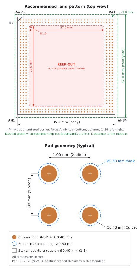
Table: Land Pattern Parameters
| Parameter | Symbol | Value | Unit |
|---|---|---|---|
| Pad pitch (signal grid) | p | 1.0 | mm |
| Copper pad diameter | — | 0.40 (dia.) | mm |
| Pad type | — | Round, NSMD | — |
| Solder-mask opening diameter | — | 0.50 (dia.) | mm |
| Stencil aperture (1:1) | — | 0.40 (dia.) | mm |
| Stencil material | — | Nano-coated steel mesh | — |
| Stencil thickness (recommended) | t | 0.08 | mm |
Keep-Out Zones
Two keep-out regions apply, both shown in Land Pattern:
- Internal keep-out — do not place components on the carrier board directly beneath the module, inside the LGA pad ring. Signal routing beneath the module is permitted, on the top layer between pads and on inner layers. Where additional clearance is required, an internal cutout in the carrier PCB under the module is permitted.
- External keep-out (courtyard) — keep a 1.0 mm component-free clearance around the module perimeter (37.0 × 37.0 mm overall) for placement tolerance, inspection, and rework access.
RF traces (especially the antenna feed) must be routed away from high-current digital paths.
Module Marking
Each module is laser-marked on the top side with the following fields:
- Manufacturer logo (Alp Lab)
- Product name:
E1M-AEN - Production date code (YYWW)
- Serial number
The full MPN is not marked on the module. Wireless regulatory marks (FCC ID, ISED IC, MIC, etc.) are carried on the on-board wireless module, not on the E1M-AEN SoM.
Packaging
Trays
The E1M-AEN is supplied exclusively in JEDEC-compliant matrix trays. Tape & reel is not offered for this module.
Tray Drawing (figure pending)
Table: Tray Specifications
| Parameter | Symbol | Value | Unit |
|---|---|---|---|
| Tray standard | — | JEDEC matrix tray | — |
| Units per tray | — | TBD | pcs |
| Trays per dry-pack bag | — | TBD | pcs |
MSL & Handling
The E1M-AEN is classified to Moisture Sensitivity Level (MSL) TBD per IPC/JEDEC J-STD-020. Modules are shipped in dry-pack with desiccant and a humidity-indicator card.
After opening the dry-pack:
- Floor life: TBD hours at ≤ 30 °C / ≤ 60% RH.
- If floor life is exceeded before reflow, bake at TBD °C for TBD h before assembly.
Refer to IPC/JEDEC J-STD-033 for full moisture/reflow handling procedures.
Ordering Information
MPN Decoder
Table: E1M-AEN MPN Convention
| Field | Example | Description |
|---|---|---|
| Family | E1M | Edge-1 AI Module standard footprint. |
| Product line | AEN | Alif Ensemble. Other product lines are denoted by different three-letter codes (e.g. V2N for STM32MP25). |
| SoC variant | 7 | Last digit of the Ensemble variant (Ex). |
| Memory option | 0 | Reserved for memory-config index; 0 = on-die memory only. |
| Assembly variant | 1 | Customer configuration code: selects which optional components are populated (e.g. wireless module, Ethernet PHY, CAN PHY, camera LDOs, connectors). 1 is the standard build; contact Alp Lab for custom assembly variants. |
Note: Example: E1M-AEN701 = E1M form factor, Alif Ensemble line, E7 SoC, on-die memory only, standard assembly variant 1.
Ordering Matrix
Table: Ordering Information
| MPN | Main CPU | RAM int. | AP cores (A32) | NPU (Ethos U55 / U85) | ISP / JPEG |
|---|---|---|---|---|---|
| E1M-AEN701 | AE722F80F55D5LS | 13.5 MB | 2 × 800 MHz | 1 × 46 GOPS + 1 × 204 GOPS | No |
| E1M-AEN501 | AE512F80F55D5LS | 13.5 MB | 1 × 800 MHz | 1 × 46 GOPS + 1 × 204 GOPS | No |
| E1M-AEN301 | AE302F80F55D5LE | 13.5 MB | — | 1 × 46 GOPS + 1 × 204 GOPS | No |
| E1M-AEN801 | AE822FA0E5597LS0 | 9.75 MB | 2 × 800 MHz | 1 × 46 GOPS + 2 × 204 GOPS | Yes |
| E1M-AEN601 | AE612FA0E5597LS0 | 9.75 MB | 1 × 800 MHz | 1 × 46 GOPS + 2 × 204 GOPS | Yes |
| E1M-AEN401 | AE402FA0E5597LE0 | 9.75 MB | — | 1 × 46 GOPS + 2 × 204 GOPS | Yes |
All configurations above include:
- 5.5 MB internal MRAM; no external OSPI memory
- Real-time cores: 1 × 160 MHz + 1 × 400 MHz Cortex-M55
- Operating temperature: − 40 °C to +85 °C
- Dual-band (2.4 GHz / 5 GHz) Wi-Fi 6 + BLE 5.4 combo module (BDE-BW3551N)
- 100 Mbit Ethernet PHY
- Display backlight driver
- 2 LDOs for external cameras
RoHS-compliant. Contact Alp Lab for custom assembly variants (lead finish, ball material, etc.).
References & Related Documents
Table: Related Documents
| Ref. | Title | Source |
|---|---|---|
| [1] | Alif Semiconductor Ensemble Series Datasheet | Alif Semiconductor |
| [2] | Alif Semiconductor Ensemble Series Reference Manual | Alif Semiconductor |
| [3] | E1MTM Specification | github.com/alplabai/e1m-spec |
| [4] | E1M-AEN Hardware Design Guide | Alp Lab (HG-AEN-001) |
| [5] | Alp SDKTM Repository | github.com/alplabai/alp-sdk |
| [6] | Alp SDKTM Documentation | docs.alplab.ai |
| [7] | Alp SDKTM VS Code Extension | github.com/alplabai/alp-sdk-vscode |
| [8] | Alp Lab Community Forum | community.alplab.ai |
| [9] | BDE-BW3551 Wi-Fi 6 / BLE Module Datasheet | BDE Technology |
| [10] | IPC/JEDEC J-STD-020 — Reflow Profile | JEDEC |
| [11] | IPC/JEDEC J-STD-033 — Moisture/Reflow Handling | JEDEC |
Revision History
Table: Revision History
| Revision | Changes | Date |
|---|---|---|
| 0.1 | Initial draft. | December 2025 |
| 0.2 | Memory options updated with the correct diagram. Wi-Fi throughput updated to 20 Mbps. | April 2026 |
| 0.3 | SoM-typical sections added: Recommended Operating Conditions, ESD & Latch-up, Thermal Characteristics, Power Sequence, Boot Modes, Reset & Module Enable, JTAG/SWD Debug, Wireless RF & Regulatory, Environmental & Reliability, Software Support, Reference Schematic, Compliance, Land Pattern, Packaging (Trays), MPN Decoder, References, Legal Notices. | May 2026 |
| 0.4 | Pin tables regenerated and verified against the E1M specification and the production board netlist (all 312 pads). Corrected power pins (VIO_OUT, MODULE_EN/STBY); removed non-existent IO_EN and +3V3_OUT; unused standard pins named "leave floating". Wireless module identified as dual-band BDE-BW3551N (CC3551E) with measured RF characteristics. USB 2.0 corrected to the USB2 pins. +V_CAM rails documented as adjustable TLV77201 LDOs. Ordering Matrix simplified; MPN decoder last field corrected to Assembly variant. Updated repository / documentation / contact links. On-module interface ESD/EMI protection removed except on the SDIO / SD-card interface; carrier board must now provide ESD/EMI protection on Ethernet, MIPI DSI, and MIPI CSI. Reflow profile populated (Pb-free, ALPHA OM338, peak 241–244 °C); SMT stencil specified (nano-coated steel mesh, 0.08 mm). Pin-out drawing redrawn as a top-view, colour-coded 312-pad diagram. | June 2026 |
| 0.5 | Pin tables re-verified against the production board netlist (E1M-AEN 2626-R2, all 312 pads). IO21 (L3) and IO22 (M3) moved from the Digital Pins table to Not-connected Pins — both pads are unbonded on E1M-AEN, like IO23– IO25. Module Output Rails: corrected VIO_OUT pins from AC1/AC2 (GND) to P1/P2. | June 2026 |
| 0.6 | Corrected NPU configuration in the key-features list: E4/E6/E8 carry 2 × Ethos-U55 + 1 × Ethos-U85 (previously mislisted as 3 × Ethos-U55). Verified against the Alif E4/E6/E8 datasheets (454 GOPS total: 46 + 204 + 204). Ordering-table NPU column relabelled "Ethos U55 / U85" to reflect the Ethos-U85 (NPU-HG) on the E4/E6/E8 parts. | July 2026 |
| 0.7 | Cover page: replaced the block-diagram placeholder with front/back product photos of the E1M-AEN module (rev 1726-R4A). | July 2026 |
| 0.8 | Cover page: added "open-source Edge-1 AI Module" sub-heading; resized cover photos so the Applications section fits on page 1. Absolute Maximum Ratings: added CAN bus (± 58 V), Ethernet MDI (− 0.3 to +4 V), and backlight boost switch node (− 0.3 to +40 V) rows. Removed the duplicated module-supply-voltage row from Electrical Characteristics (retained in Recommended Operating Conditions). Documented interface ESD protection: Ethernet DP83825I (± 5 kV IEC 61000-4-2), CAN TCAN1044AVDRBRQ1 (ISO 10605 ± 8 kV contact / ± 15 kV air), SD-card NVT4858HKZ (IEC 61000-4-2 level 4, ± 8 kV / ± 15 kV). Named the backlight controller (KTD2801ECD-TR, 36 V OVP). | July 2026 |
| 0.9 | Recommended Operating Conditions and Environmental Conditions: removed the S/E temperature grades and the +105 °C E-grade and junction-operating rows; the module is now specified over a single − 40 °C to +85 °C ambient range. Power Architecture: clarified that no power-rail sequencing is required (PMIC-managed rail bring-up), separate from the carrier-side control-signal bring-up steps in the Power-Up & Reset Sequence. MIPI CSI Camera: added an "On-die ISP & JPEG Encoder (E4 / E6 / E8)" subsection detailing the Ensemble ISP and JPEG-encoder feature sets (verified against the Alif E8 datasheet v1.0 §3.19.3–3.19.4); noted the blocks are absent on E3 / E5 / E7 and not yet exposed through the Alp SDK. MIPI DSI / CSI: stated interface throughput and resolution (DSI 2-lane × 1.25 Gbps, up to FHD; CSI-2 2-lane × 2.5 Gbps, up to 2 MP) and added a MIPI Interface Summary table (verified against the Alif E8 datasheet v1.0). | July 2026 |
| 0.10 | MIPI DSI Display: removed the incorrect "up to FHD (1080p)" display-resolution claim. The Alif E8 datasheet v1.0 (§3.20.2) specifies no fixed DSI panel resolution — the maximum is limited by the pixel clock and the 2-lane × 1.25 Gbps D-PHY Tx link bandwidth (video mode only). The 1920 × 1080 (2 MP) figure applies to the ISP / camera-input path, not the DSI display output. DSI lane rate (1.25 Gbps/lane, 2.5 Gbps aggregate) re-confirmed correct against the datasheet. | July 2026 |
Legal Notices
Disclaimer
The information in this document is provided in connection with Alp Lab AB products. No license, express or implied, by estoppel or otherwise, to any intellectual property right is granted by this document. Alp Lab reserves the right to make corrections, modifications, enhancements, improvements, and other changes to its products and services at any time without notice.
Alp Lab products are not authorised for use as critical components in life-support devices, safety-critical equipment, military applications, or any other application where failure of the product could reasonably be expected to result in personal injury or significant property damage, without the express written approval of an officer of Alp Lab AB.
Trademarks
Alp Lab, Alp SDK™, E1M™, and the Alp Lab logo are trademarks of Alp Lab AB. Arm, Cortex, and Ethos are trademarks of Arm Limited. Alif Semiconductor and Ensemble are trademarks of Alif Semiconductor. All other trademarks are the property of their respective owners.
Export Control
This product may be subject to export-control regulations. The customer is responsible for complying with all applicable export-control laws.
Contact
For sales, technical support, or custom-variant requests:
- Web: alplab.ai
- Email: contact@alplab.ai
- Repository: github.com/alplabai
- Documentation: docs.alplab.ai
- Community: community.alplab.ai