E1M-AEN HW Design Guide
Introduction
Purpose of This Document
This Hardware Design Guide provides practical guidance for developers and system integrators designing a carrier board for the E1M-AEN System-on-Module (SoM).
It covers:
- Hardware integration and carrier board design
- Power architecture and system bring-up
- Interface usage and pin functional intent
- Common pitfalls during first implementation
This guide complements:
- The E1M-AEN Datasheet
- Alif Semiconductor Ensemble SoC documentation
- Alp SDKTM documentation
Product Overview
The E1M-AEN is a compact 35 × 35 mm Edge-AI System-on-Module, based on the Alif Semiconductor Ensemble series, targeting industrial, IoT, robotics, and low-power AI applications.
The module follows the E1MTM open-standard pin layout, enabling drop-in compatibility across the E1M series without redesigning the carrier board.

Key characteristics:
- Unified pinout across multiple MCU/MPU variants
- On-module power management; interface EMI/ESD protection is provided on the carrier board (except the SD-card interface, which is protected on-module)
- Single external 5 V supply
- Long-term lifecycle orientation
Supported SoC Variants
Table: SoC Variants
| Variant | Application CPU | Real-Time CPU | NPU |
|---|---|---|---|
| E3 | — | 2 × Cortex-M55 | 2 × Ethos-U55 |
| E5 | 1 × Cortex-A32 | 2 × M55 | 2 × Ethos-U55 |
| E7 | 2 × Cortex-A32 | 2 × M55 | 2 × Ethos-U55 |
| E4 | — | 2 × Cortex-M55 | 2 × Ethos-U55 + 1 × Ethos-U85 |
| E6 | 1 × Cortex-A32 | 2 × M55 | 2 × Ethos-U55 + 1 × Ethos-U85 |
| E8 | 2 × Cortex-A32 | 2 × M55 | 2 × Ethos-U55 + 1 × Ethos-U85 |
Note: Firmware images must match the installed Ensemble variant.
Mechanical Information
Dimensions
- Size: 35 × 35 mm
- Form factor: Connectorless, solder-down LGA SoM
- Mounting: Land-grid-array (LGA) pads, reflowed directly onto the carrier board
The complete mechanical drawing (dimensions, tolerances, height, and mass) is in the E1M-AEN Datasheet. The values below are the subset a carrier-board designer needs to lay out the footprint.
Land Pattern
Design the carrier-board footprint to the recommended land pattern below. The module uses a 1.0 mm pad grid with 0.4 mm round, non-solder-mask-defined (NSMD) pads, following IPC-7351 nominal density for LGA packages.
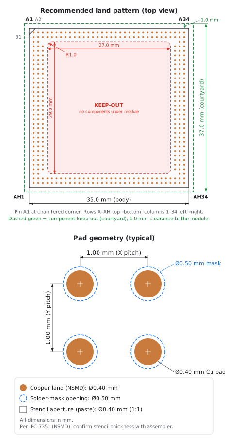
Table: Land Pattern Parameters
| Parameter | Value | Unit |
|---|---|---|
| Pad pitch (signal grid) | 1.0 | mm |
| Copper pad diameter | 0.40 (dia.) | mm |
| Pad type | Round, NSMD | — |
| Solder-mask opening diameter | 0.50 (dia.) | mm |
| Stencil aperture (1:1) | 0.40 (dia.) | mm |
| Stencil material | Nano-coated steel mesh | — |
| Stencil thickness (recommended) | 0.08 | mm |
Tip: A 4-layer (or denser) carrier board is recommended so that signals can be routed out from under the module on inner layers without crowding the top-layer escape routes.
Keep-Out Zones
Two keep-out regions apply:
- Internal keep-out — do not place components on the carrier directly beneath the module, inside the LGA pad ring. Signal routing beneath the module is permitted on the top layer between pads and on inner layers. Where extra clearance is needed, an internal cutout in the carrier PCB under the module is allowed.
- External keep-out (courtyard) — keep a 1.0 mm component-free clearance around the module perimeter (37.0 × 37.0 mm overall) for placement tolerance, inspection, and rework access.
Note: Route the RF antenna feed (AH1) away from high-current digital paths, and keep the carrier-board ground pour clear of any on-module or carrier antenna keep-out. See Wi-Fi and BLE.
Handling and Assembly
- ESD-sensitive device — use grounded handling equipment
- Avoid mechanical stress after soldering
- Follow standard reflow and PCB flatness rules
- Observe the module's Moisture Sensitivity Level (MSL) and dry-pack floor life; bake before reflow if floor life is exceeded (see the datasheet MSL & Handling section)
- The module is supplied in JEDEC matrix trays (no tape & reel)
PCB Layout Guidelines
Layer Stack-Up
The E1M-AEN exposes several controlled-impedance interfaces (100 Ω differential Ethernet and MIPI, 90 Ω differential USB 2.0, and 50 Ω single-ended RF). A minimum 4-layer carrier board is recommended; 6 layers eases escape routing and gives cleaner reference planes for high-speed pairs. A typical 4-layer stack-up is:
Table: Reference 4-Layer Stack-Up
| Layer | Use | Notes |
|---|---|---|
| L1 (top) | Signal + components | High-speed escapes, RF trace, module pads |
| L2 | Ground plane | Solid, unbroken reference for L1/L3 high-speed pairs |
| L3 | Power + low-speed signal | Split power pours; keep high-speed off this layer |
| L4 (bottom) | Signal + ground pour | Slow signals, additional ground stitching |
Tip: Reference every high-speed pair to a continuous ground plane (L2). Never route a differential pair across a plane split — the return current cannot follow and emissions/cross-talk rise sharply.
Controlled-Impedance Routing
Set the dielectric heights and trace geometry with your fabricator's impedance calculator to hit the targets below. Match lengths within each pair first (intra-pair skew), then across pairs of the same bus (inter-pair skew).
Table: Impedance & Skew Targets
| Interface | Impedance | Tolerance | Length matching |
|---|---|---|---|
| Ethernet (10/100) | 100 Ω diff | ± 10% | Intra-pair ≤ ± 2 ps |
| MIPI CSI-2 / DSI | 100 Ω diff | ± 10% | Intra-pair tight; match clock to data lanes in the group |
| USB 2.0 HS | 90 Ω diff | ± 10% | Intra-pair ≤ ± 5 ps |
| RF antenna feed | 50 Ω single-ended | ± 10% | — |
- Keep high-speed pairs short and direct; minimize vias (each via is an impedance discontinuity) and avoid stubs.
- Where a pair must change layers, place ground stitching vias adjacent to the signal vias to give the return current a path.
- Keep digital switching noise and high-current paths away from analog, RF, and MIPI routing.
Power Architecture
Power Input
- Input voltage: 5 V DC nominal (single rail) on the
VDDINpads (R1, S1, R2, S2) - Recommended range: 4.5 V – 5.5 V
- Absolute maximum: 6.0 V (do not exceed; see datasheet Absolute Maximum Ratings)
- All regulators, the PMIC, and power sequencing are on-module — no external sequencing is required
No additional input power rails must be supplied. Size the 5 V source for the worst-case peak current of the chosen Ensemble variant plus any current drawn from the module's output rails (below).
Module Output Rails
The module generates these regulated rails back to the carrier from the 5 V input. Budget current carefully — they are intended for light carrier-side loads and on-module camera power, not for powering large external subsystems.
Table: Module Output Rails
| Rail | Pins | Voltage | Max | Purpose |
|---|---|---|---|---|
| VIO_OUT | P1, P2 | 1.8 V ± 5% | 200 mA | I/O reference for carrier-side level shifters / pull-ups. |
| +V_CAM0 | Z34 | 0.6 – 3.3 V (adj.) | 300 mA | Adjustable LDO (TLV77201), set via CAM_VFB0. Camera rail or light carrier load. |
| +V_CAM1 | AB34 | 0.6 – 3.3 V (adj.) | 300 mA | Adjustable LDO (TLV77201), set via CAM_VFB1. Camera rail or light carrier load. |
Warning: Do not power external loads from the SoM output rails unless the load has been validated against the current limits above.
Power Design Guidelines
- Place bulk capacitance (e.g. 10 µF) plus a 100 nF decoupling capacitor close to the
VDDINpads. The module includes its own internal decoupling; carrier-side caps improve transient response. - Use a solid, low-impedance ground plane and connect all GND pads to it.
- Keep the 5 V high-current paths short and wide.
- If a buck converter feeds
VDDIN, confirm it can supply the SoM's load transients, not just the average current.
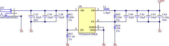
A buck converter can be used to create 5 V for the SoM. Make sure the selected buck converter can support the load transients of the SoM. The E1M development board generates its rails with TI TLV62595DMQR (4 A) and TI TPS564247DRLR (6 A) step-down converters.
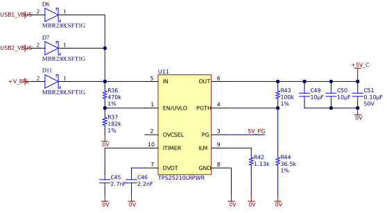
Additionally, the user can add power ORing using diodes or eFuses. In this case, the input power is multiplexed. The E1M development board uses a TI TPS25210LRPWR eFuse for input protection (with Schottky diodes for ORing of redundant supplies).
Power-Up & Reset Sequence
No power-rail sequencing is required — the on-module PMIC handles rail bring-up. The recommended carrier-side control-signal bring-up order is:
- Apply 5 V to
VDDIN. - Release
MODULE_EN(let the internal pull-up hold it high). - Release
PORn(let the internal pull-up hold it high). - Wait for the on-module rails to stabilise and the SoC boot ROM to start.
- Begin communication with the module.
For power-down, drive MODULE_EN low and remove VDDIN; no controlled power-down sequence is needed at the carrier level. Refer to the datasheet Power-Up & Reset Sequence for the module-level timing diagram.
Carrier Control Signals
Expose these control pins on the carrier as needed:
Table: Carrier Control Signals
| Pin | Direction | Description |
|---|---|---|
MODULE_EN (O1) | Input, open-drain | Internally pulled up to VDDIN. Pull low to disable the module; leave floating if unused. |
PORn (W1) | Input, open-drain | Internally pulled up to 1V8. Pull low for a power-on reset. Optionally fit a reset push-button between PORn and GND. |
MODULE_STBY (O2) | Input, open-drain | Internally pulled up to 1V8. On E1M-AEN, stand-by is supported only for the real-time clock. Leave floating if unused. |
Memory and Boot Architecture
Internal Memory (SoC-Dependent)
- SRAM: 128 KB – 13.5 MB
- MRAM: 256 KB – 5.5 MB
On Board Memory (ON SoM)
- OSPI interfaces supported
- Configurable for RAM or ROM. Either of them can be RAM or ROM.
- Configuration depends on E1M variant.
Note: Contact Alp Lab for additional information and configuration.
BOOT
BOOTpin functionality is not supported on E1M-AEN. Alif SoCs have no boot-mode strap pins; leaveBOOT0–BOOT3floating.- The boot ROM loads the application image from internal MRAM. External boot sources (OSPI flash, SD card) are selected in software once the boot ROM is running.
- For
MODULE_ENandMODULE_STBYcarrier wiring, see the Carrier Control Signals table in the Power Architecture section.
JTAG / SWD Debug
Expose the module's 5-pin JTAG/SWD interface on the carrier for programming and debug. Signals operate at 1.8 V — add carrier-board level shifters if your debug probe drives 3.3 V.
Table: JTAG / SWD Pinout
| Pin | Signal | Description |
|---|---|---|
| X1 | JTAG_TCK / SWDCLK | Test clock (JTAG) or serial-wire clock (SWD). |
| X2 | JTAG_TDI | Test data in (JTAG only). |
| Y1 | JTAG_TMS / SWDIO | Test mode select (JTAG) or serial-wire I/O (SWD). |
| Y2 | JTAG_TDO | Test data out (JTAG only). |
| Z1 | JTAG_nRST | Active-low reset to the SoC debug logic. |
Tip: Bring the JTAG/SWD signals out to a standard 10-pin 1.27 mm Cortex debug header (e.g. Samtec FTSH-105). The E1M development board uses this footprint.
Carrier Board Reference Block Diagram
The carrier board has been designed around the E1MTM open standard to support all E1M variants. Note that E1M-AEN does not implement every peripheral available in the full E1MTM pinout (e.g. PCIe, the second Ethernet/CSI/DSI, and USB SuperSpeed are not bonded) — see the datasheet Not-connected Pins table.
E1M-AEN carrier board reference block diagram (figure pending)
System-Level Overview
The carrier board provides:
- 5 V power input and protection
- External connectors and signal conditioning
- Application-specific peripherals
All complex power, RF, EMI, and processing functions are integrated into the E1M-AEN module.
Design Philosophy
- Keep the carrier board simple and application-specific
- Avoid duplicating functionality already on-module
- Enable reuse across Ensemble variants
- Minimize RF, power, and EMI risk on the carrier board
Interfaces Overview
All interfaces are exposed through the standardized E1MTM pinout. The pin-out drawing below shows the pad locations; the full per-pin tables (Power & Control, Analog, Digital, Not-connected, Reserved) are in the E1M-AEN Datasheet and are the authoritative reference for carrier layout.
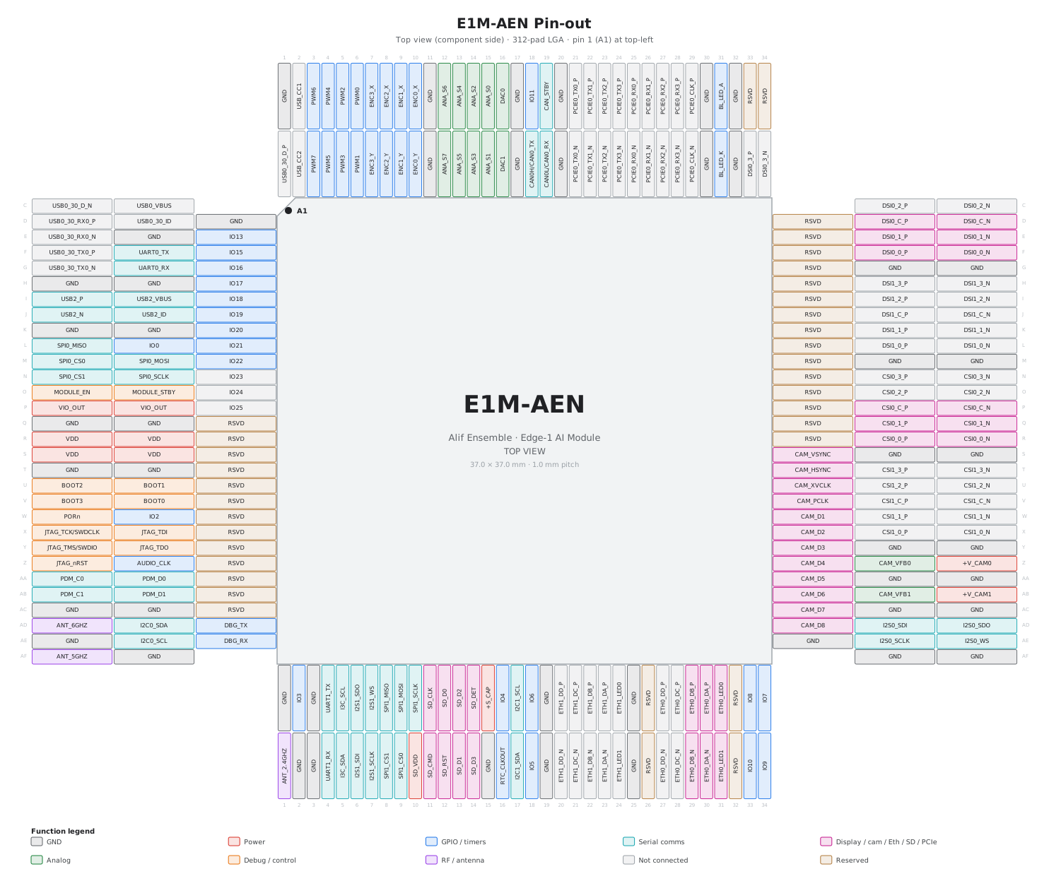
Note: Check the E1M-AEN datasheet and the E1MTM specification for the authoritative pin map and electrical limits. Pins can be reassigned to alternate functions in software, but hardware compatibility with other E1M variants then no longer holds.
Ethernet Interface
- 100 Mbps Ethernet via on-module PHY (TI DP83825I)
- External magnetics and RJ45 required
- Auto-negotiation enabled
- EMI/ESD protection required on the carrier board
Route ethernet lines with 100 Ω in differential pairs. Make sure the match the length within each pair with ± 2 ps tolerance. The module does not integrate Ethernet ESD/EMI protection — add a low-capacitance ESD/TVS array (and common-mode choke as needed) on the MDI lines between the magnetics and the connector.
The E1M development board uses an Abracon ARJM11C7-502-KB-EW2 integrated-magnetics RJ45 jack (2 kV isolation); any equivalent 10/100 magnetics jack with the same pinout may be substituted.
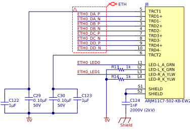
Note: Ensemble Series supports only 1 ethernet interface. Hence only primary ethernet interface can be used on the SoM.
Wi-Fi and BLE
- Dual-band (2.4 GHz / 5 GHz) Wi-Fi 6 and BLE 5.4 via BDE-BW3551N module (TI CC3551E)
- External antenna required
- Impedance-controlled RF routing
- Keep digital noise away from RF paths
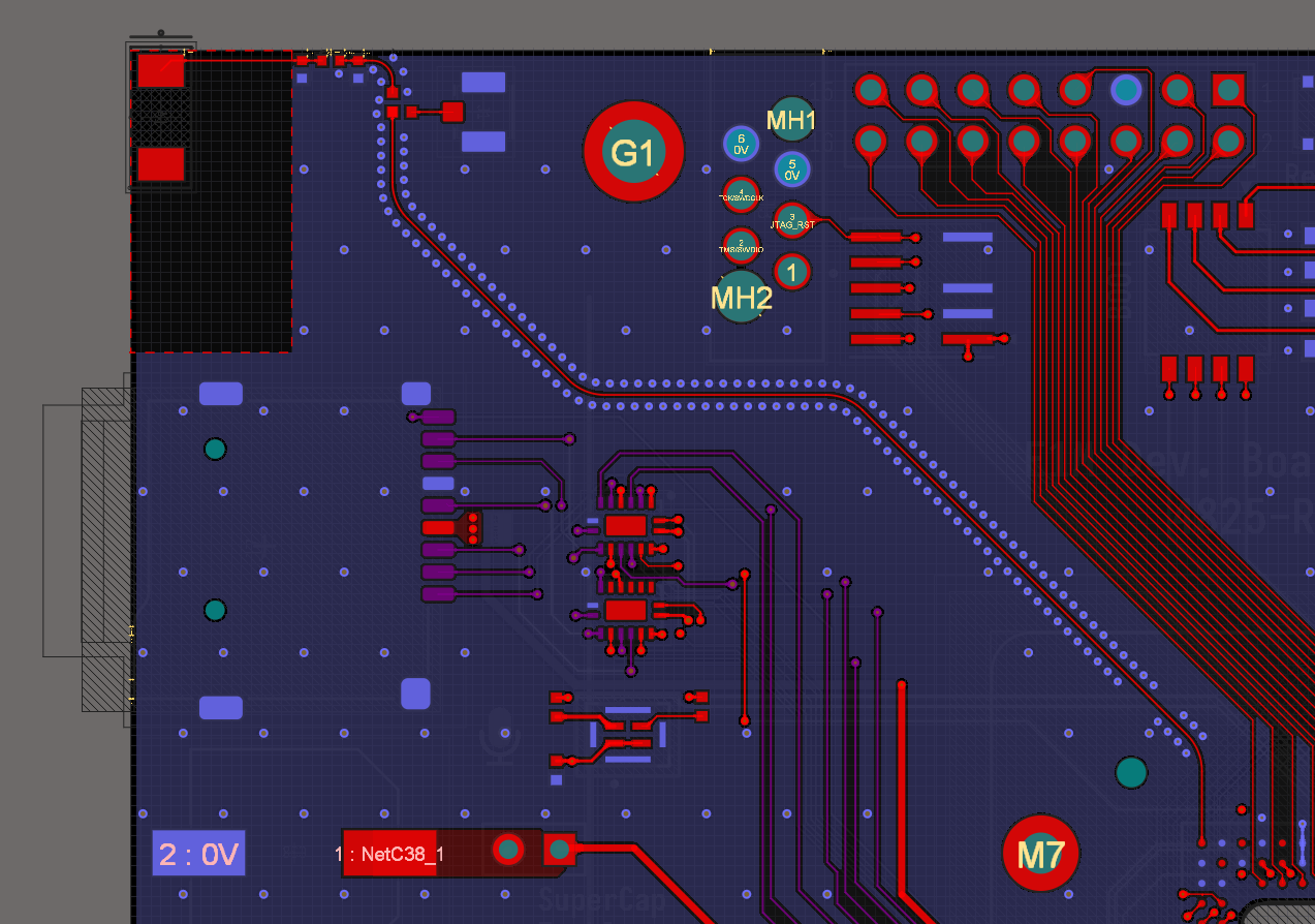
The module's combined antenna feed is brought out on the ANT_2.4GHZ pad (AH1). It can be routed three ways:
- On-module U.FL connector — connect an external antenna directly to the module.
- Carrier-board PCB / chip antenna — route AH1 out as a 50 Ω controlled-impedance trace to an antenna on the carrier.
- Carrier-board RF connector — extend the 50 Ω trace to a U.FL / IPEX / SMA connector.
The separate ANT_5GHZ (AF1) and ANT_6GHZ (AD1) pads are not used on E1M-AEN (the BDE-BW3551N uses a single combined port) — leave them floating.
Route the RF trace with 50 Ω impedance, keep it short and away from noise sources and other components, and add via shielding (a ground fence) along the trace. Follow the antenna vendor's design guidelines.
The E1M development board feeds the RF output through a Samtec RSP-122811-01 U.FL connector and a 3-element π-matching network (Murata LQW15AN22NH, 22 nH) to an Ignion NN02-201 multiband chip antenna (4.1 dBi, 824 MHz – 7.125 GHz). Populate the matching network footprints and tune per the antenna vendor's guidelines.
Warning: The on-module wireless certifications apply only when the module is used with a certified antenna. Using an unlisted antenna voids the modular grant and requires re-certification on the end product. See the datasheet Regulatory Information.
MIPI CSI-2 Camera
- Single-camera support
- 2-lane MIPI CSI-2
- Controlled-impedance differential routing
- Minimize vias and stubs
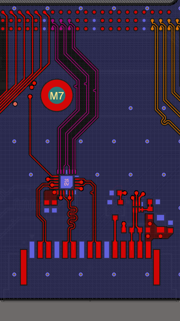
Ensemble series has one CSI-2 interface for a camera input. The traces must be routed as 100 Ω ± 10% differential. Make sure the match the lengths within the pairs and the group.
Protect the CSI lanes with a low-capacitance TVS array (the E1M development board uses Semtech RCLAMP3552T.TNT). Where a single CSI port is shared between multiple camera connectors, the development board switches the lanes with a Diodes PI3WVR626XEBEX MIPI mux.
Camera power. The module's two adjustable LDO rails (+V_CAM0 / +V_CAM1, TLV77201) can supply the camera directly, avoiding a carrier-side regulator. Set each output with an external divider on the CAM_VFBx feedback pin, placed as close to the pin as possible:
VCAM = 0.6 V × (1 + R1 / R2)
To keep feedback-pin current error small, size the divider for ~ 100 × the maximum feedback-pin current (IFB,max = 100 nA), i.e. R1 + R2 ≤ VOUT / (IFB × 100).
MIPI DSI Display
- 2-lane MIPI DSI
- Up to Full HD
- Display power managed externally
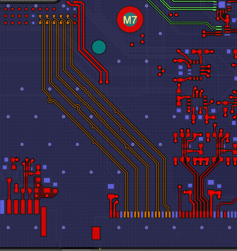
Ensemble series has one DSI interface for a display output. The traces must be routed as 100 Ω ± 10% differential. Make sure the match the lengths within the pairs and the group.
Protect the DSI lanes with a low-capacitance TVS array (the E1M development board uses Semtech RCLAMP3552T.TNT). High-speed lane switching to multiple display connectors is handled on the development board by a Diodes PI3DBS12212AXUAEX differential mux.
Backlight. The module includes an optional backlight LED driver (up to 10 LEDs in series, or 2P6S), controlled by the Alp SDKTM via the BL_LED_A (anode) and BL_LED_K (cathode) pins. Set the LED current with the feedback resistor:
ILED = 95 mV / RFB
If the on-module driver is not used, the BL_PWM signal can instead be exposed directly to drive an external backlight driver; leave BL_LED_K floating in that case.
CAN-BUS
- Optional on-module CAN PHY (TI TCAN1044AVDRBRQ1), populated per assembly variant
- When the on-module PHY is fitted: only termination, ESD, and EMI protection are needed on the carrier
- When it is not fitted: add a CAN transceiver on the carrier (the E1M EVK uses a TI TCAN1044AVDRBRQ1)
Add ESD protection and termination resistors. The E1M development board (whose module variant does not populate the on-module CAN PHY) carries its own TI TCAN1044AVDRBRQ1 transceiver, protected by a Nexperia PESD2IVN24-UX TVS diode and a Murata DLW43SH510XK2L common-mode choke between the transceiver and the connector.
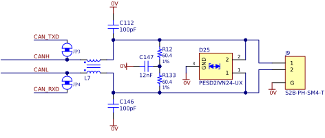
Note: The CAN-BUS transceiver is optional on E1M. If isolation desired, external transceiver must be used.
USB 2.0
- One USB 2.0 interface, Full-Speed (12 Mbit/s) and High-Speed (480 Mbit/s)
- Host or device operation
- Brought out on the E1M standard
USB2pins (I1/J1)
Route USB2_P / USB2_N (I1/J1) as a 90 Ω differential pair. Wire the role and power pins as follows:
Table: USB 2.0 Connections
| Pin | Signal | Description |
|---|---|---|
| I1 / J1 | USB2_P / USB2_N | 90 Ω differential data pair. |
| J2 | USB2_ID | Low: host mode. NC: device mode. |
| I2 | USB2_VBUS | Connect to USB VBUS 5 V. |
Note: The standard
USB0pins (B1/C1/...) carry the optional USB 3.x SuperSpeed lanes, which are not used on E1M-AEN. Leave them floating.
SD Card / eMMC
- One SDIO interface for an external µSD card or eMMC
- On-module ESD protection and 33 Ω series resistors on the SDIO lines
- Card power supplied from the module's
SD_VDD(AH10) output
Add only the card connector (and optional card-detect wiring) on the carrier; no additional series termination or ESD is required on the SDIO lines.
Digital Communication
- UART, SPI, I2C / I3C
- Pin-mux configured in software
- I2C/I3C typically require pull-ups
- SPI chip-selects handled on carrier board
E1M uses a dedicated pin out, the user needs to use the relevant functions in the application.
Audio and Sensor Interfaces
- I2S and PDM
- Digital microphones and codecs
- Keep clocks clean and isolated
Analog Interfaces
- ADC: 8 channels, 12-bit, up to 5 Msps, referenced to 1V8
- DAC: 2 channels, 12-bit, 1 kHz, referenced to 1V8
- Keep analog routing short and isolated from digital/RF switching
- An optional 0.1% standalone 1V8 reference is available on E1M
PWM and Encoder Interfaces
- 8 × PWM outputs
- 4 × encoder inputs
- Suitable for motor and control use
- Software configuration required
Thermal Design
The E1M-AEN dissipates heat primarily through the Ensemble SoC into the module PCB and, from there, into the carrier board. The SoC package thermal-resistance figures (θJA ~ 21 °C/W still air, θJC ~ 17 °C/W) are listed in the datasheet; the realised thermal performance depends heavily on how the carrier board pulls heat away. Maximum junction temperature is +105 °C operating (+150 °C absolute).
Carrier-board measures that improve thermal performance:
- Copper area — provide generous ground/power copper pours on inner and bottom layers beneath and around the module to spread heat.
- Via stitching — stitch the ground pads under the module to inner planes with a dense via array to conduct heat into the board.
- Airflow — even modest forced airflow significantly lowers θJA; account for enclosure ventilation early.
- Derating — above +85 °C ambient, derate the AI workload / clock to stay within TJ,max. Worst-case dissipation occurs during sustained NPU inference with Wi-Fi TX active.
Tip: For sustained full-clock AI workloads in still air, validate junction temperature against your enclosure early — copper area and via stitching under the module are the cheapest and most effective levers.
Software Support
Alp SDKTM
- Open-source, CMSIS-compliant
- Unified HAL across E1M variants
- Vendor-agnostic software architecture
AI Acceleration
- Integrated Arm Ethos-U55 NPU(s)
- Scales with Ensemble variant
- Optimized for low-power edge AI
Bring-Up Checklist
Pre-Power Checks
- Confirm correct SoM variant
- Verify orientation and solder joints
- Ensure only 5 V is connected
- Check ground continuity
- Confirm Ethernet magnetics populated (if used)
- Inspect MIPI routing
First Power-On
- Apply 5 V
- Monitor current consumption
- Check for abnormal heating
- Confirm stable startup
Basic Validation
- UART boot/debug output
- Ethernet link up
- GPIO or PWM toggle
- Peripheral enumeration via SDK
Common Issues
- Missing Ethernet magnetics
- Wrong firmware image
- Poor MIPI routing
- Supplying unintended rails
Design Checklist (Summary)
Table: Design checklist
| Item | Status |
|---|---|
| Single 5 V supply, bulk + decoupling at VDDIN | OK |
| All GND pads tied to a low-impedance plane | OK |
| Output-rail current budget within limits (VIO_OUT / +V_CAM) | OK |
| 4-layer+ stack-up with continuous ground reference | OK |
| Controlled impedance: 100 Ω MIPI/Ethernet, 90 Ω USB, 50 Ω RF | OK |
| Ethernet magnetics + RJ45 populated | OK |
| RF-clean antenna routing + certified antenna | OK |
| JTAG/SWD debug header exposed (1V8 level) | OK |
| Land pattern + internal/external keep-out observed | OK |
| Thermal: copper area + via stitching under module | OK |
| Correct firmware per variant | OK |
Ordering Information
E1M-AEN modules are ordered based on:
- Ensemble SoC variant
- Memory configuration
- Assembly options
Refer to the official ordering table for valid MPNs.
References & Related Documents
Table: Related Documents
| Ref. | Title | Source |
|---|---|---|
| [1] | E1M-AEN Datasheet (DS-AEN-001) | Alp Lab |
| [2] | E1MTM Specification | github.com/alplabai/e1m-spec |
| [3] | Alif Semiconductor Ensemble Series Datasheet | Alif Semiconductor |
| [4] | Alif Semiconductor Ensemble Series Reference Manual | Alif Semiconductor |
| [5] | BDE-BW3551 Wi-Fi 6 / BLE Module Datasheet | BDE Technology |
| [6] | Alp SDKTM Repository | github.com/alplabai/alp-sdk |
| [7] | Alp SDKTM Documentation | docs.alplab.ai |
| [8] | Alp Lab Community Forum | community.alplab.ai |
Notices
- Specifications subject to change without notice
- Some features may be preliminary
- Always verify against the latest datasheet
© Alp Lab AB. All rights reserved.
Release History
Table: Release History
| Revision | Changes | Date |
|---|---|---|
| 0.1 | Initial draft | April 2026 |
| 0.2 | Expanded to carrier-design depth: added Land Pattern & Keep-Out, PCB Layout Guidelines (stack-up + controlled-impedance/skew targets), Module Output Rails, Power-Up & Reset Sequence, Carrier Control Signals, pin-out reference, JTAG/SWD debug header, USB 2.0 and SD/SDIO interfaces, camera-LDO and backlight-driver design, Thermal Design, and a References section. Fixed status/naming/link consistency. Interface ESD/EMI protection moved to the carrier board (on-module protection retained only on the SD-card interface). Stencil spec updated (nano-coated steel mesh, 0.08 mm). Pin-out figure replaced with the top-view, colour-coded 312-pad drawing. | June 2026 |
| 0.3 | SoC Variants table: E4/E6/E8 NPU corrected to 2 × Ethos-U55 + 1 × Ethos-U85 (was 3 × Ethos-U55), per the Alif E4/E6/E8 datasheets. | July 2026 |
| 0.4 | Power-Up & Reset Sequence: reworded to separate on-module PMIC rail sequencing (no carrier-side rail sequencing required) from the carrier-side control-signal bring-up order. | July 2026 |