E1M-X V2N Datasheet
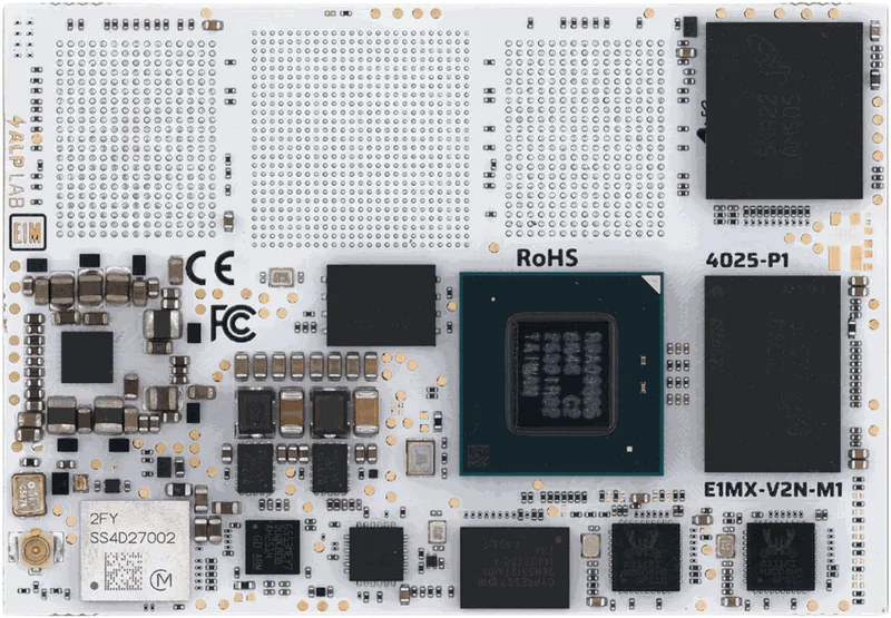
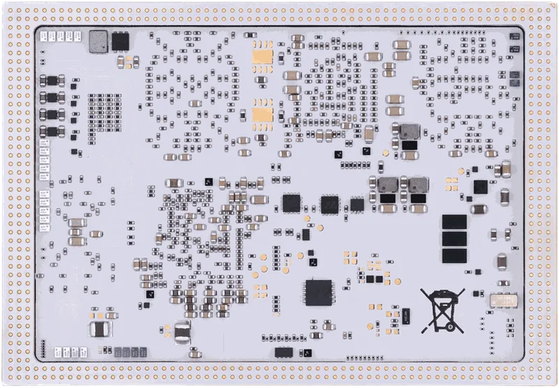
The E1M-X V2N module uses the open-source Edge-1 AI Module (E1MTM) form factor, with a unified pin layout and hardware functionality. This footprint allows users to interchange MPU modules seamlessly while keeping hardware compatible. E1MTM is designed for flexibility, functionality, and longevity in high- and medium-range MCU/MPUs.
Features
- Renesas RZ/V2N
- Quad Arm® Cortex®-A55 (1.8 GHz)
- Arm Cortex-M33 (200 MHz)
- Arm MaliTM-C55 ISP (Image Signal Processor)
- Arm MaliTM-G31 GPU
- AI Accelerator DRP-AI3 — 4 dense TOPS
- H.264 / H.265 codec
- Dedicated I/O MCU
- Arm® Cortex®-M33 (216 MHz)
- Various memory options
- LPDDR4X 32-bit 3.2 GT/s, up to 8 GB
- eMMC — 4 GB to 256 GB
- SPI NOR – 128 Mbit, boot-supported
- MIPI Display output — 4 lanes
- 1920 × 1200 RGB888 @ 60 fps
- 1280 × 1024 RGB888 @ 120 fps
- H.264 / H.265 codec
- H.264 1920 × 1080 × 60 fps
- H.265 3840 × 2160p × 30 fps
- 2 × CSI-2 camera inputs — 4 lanes, up to 4K @ 30 fps, 4 virtual channels
- 2.4 GHz / 5 GHz / 6 GHz Wi-Fi® + Bluetooth® module
- 802.11 a/b/g/n/ac/ax, 143 Mbps
- Bluetooth® 5.4 BR/EDR/LE, 3 Mbps
- 2 × 1 Gbps Ethernet PHY
- 2 × CAN-BUS PHY
- PCIe Express® 3.0 — 2 lanes
- Assembly variants available for cost reduction
- Smallest size in the industry: 45 × 65 mm
Applications
IoT, industrial, robotics, motor drive, drones, mobile PoS, smart speakers, object detection, medical devices, vending machines, smart home, process control, smart appliances, scanners.
General Description
Highlights
The Alp Lab E1M-X V2N SoM (System-on-Module) is a high-performance, cost-effective solution designed for a range of AI-driven vision applications. Powered by the Renesas RZ/V2N processor, it features an Arm® Quad Cortex®-A55 (1.8 GHz) CPU, an integrated AI accelerator, and a 4K encoder/decoder, making it optimised for vision-based tasks. The E1M-X V2N SoM supports up to two cameras via 2 × 4-lane MIPI CSI-2 connections and offers customisable options such as on-board Wi-Fi / Bluetooth, multiple memory and storage capacities, and PHY configurations.
Block Diagram
E1M-X V2N Block Diagram (figure pending)
Module Variants
The E1M-X V2N family ships in two MPN variants that share an identical pin-out and silicon stack; they differ only in the memory tier. See Ordering Information for the full ordering matrix and MPN decoder.
Table: E1M-X V2N Variant Summary
| MPN | Renesas part | LPDDR4X | eMMC |
|---|---|---|---|
| E1M-V2N101 | R9A09G056N44GBG#AC0 | 32 Gbit | eMMC 5.1, 32 Gbit |
| E1M-V2N102 | R9A09G056N44GBG#AC0 | 64 Gbit | eMMC 5.1, 128 Gbit |
Renesas RZ/V2N MPU
The RZ/V2N is a vision-AI microprocessor (MPU) with Renesas' proprietary AI accelerator (DRP-AI3) supporting up to 15 TOPS of AI performance. Its CPUs are quad Arm® Cortex®-A55 (1.8 GHz) and Arm Cortex-M33 (200 MHz). The RZ/V2N is equipped with an ISP (Image Signal Processor) and dual-channel MIPI® CSI-2® camera interfaces for supporting dual-camera signal processing, which is crucial for realising vision systems. It is also equipped with high-speed interfaces such as PCIe® and USB 3.2, allowing for the expansion of external devices. The RZ/V2N is an ideal microprocessor for applications requiring both low power consumption and advanced AI inference, such as DMS (Driver Monitoring System), monitoring cameras, mobile robots, and more.
This document should be read together with the V2N datasheet from Renesas.
Renesas RZ/V2N MPU Block Diagram (figure pending)
Key MPU features:
- Cortex-A55 (1.8 GHz) × 4 cores
- Cortex-M33 (200 MHz) × 1 core
- AI Accelerator DRP-AI
- Arm MaliTM-C55 ISP (option)
- 1.5 MB on-chip SRAM
- LPDDR4 / LPDDR4X memory interface
- Gigabit Ethernet 2 ch
- USB 2.0 interface 1 ch (Host/Function)
- USB 3.2 (Gen2) interface 1 ch (Host only)
- PCIe interface (Gen3, 2-lane) 1 ch
- MIPI CSI-2 camera interface 2 ch
- CAN interface (CAN FD) 6 ch
- AD converter 24 ch
Pin Diagram and List
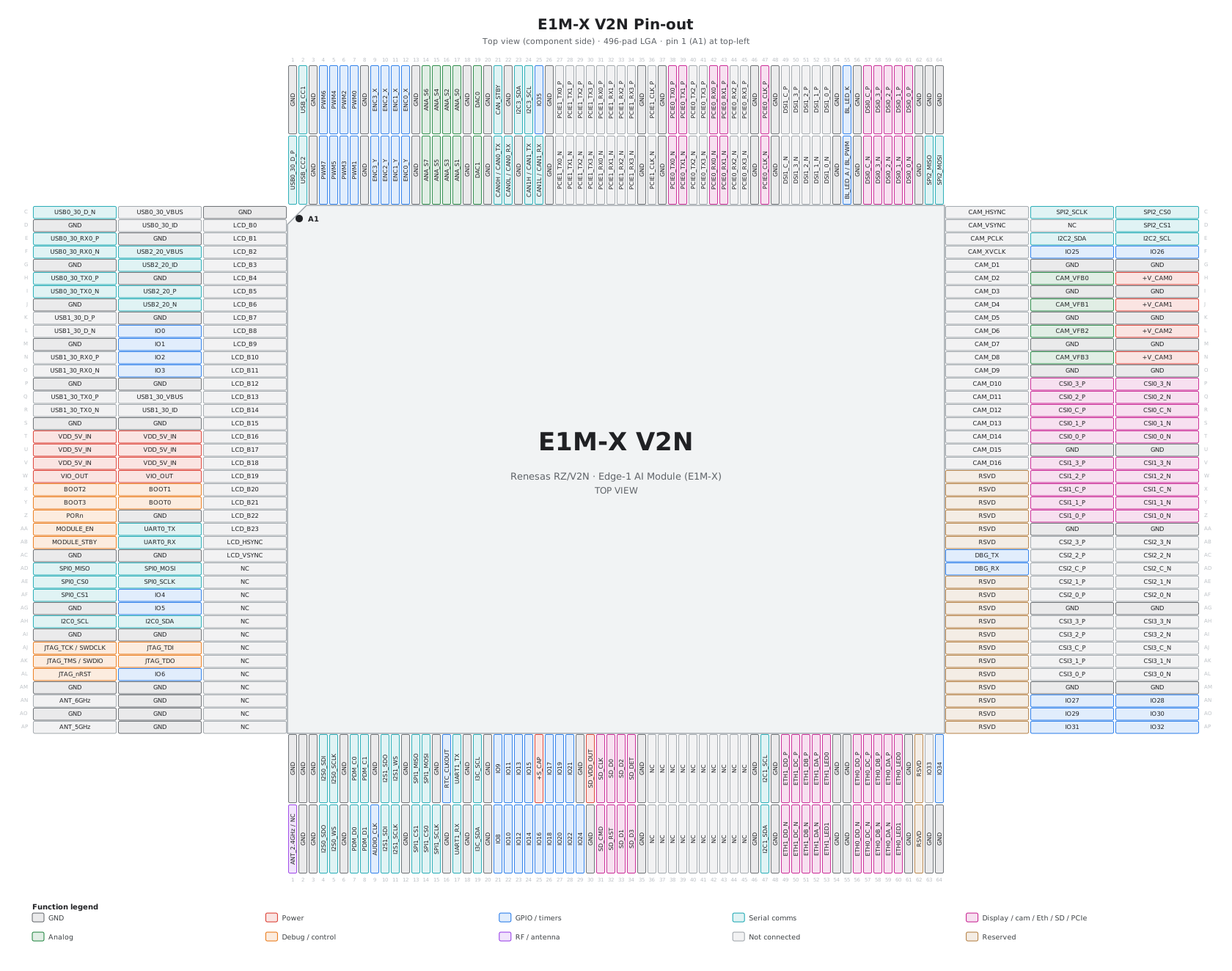
The E1M-XTM standard defines the primary pin functions; the pin-out below follows that standard. Pins can be reassigned to alternate functions in software, but hardware compatibility with other E1M-X variants will no longer hold because each MCU/MPU has a different pin structure and peripheral mapping.
Power & Control Pins
Table: E1M-X V2N Power & Control Pins
| Pin Number | Pin Name | Description |
|---|---|---|
| A13, K63, AQ15, M1, M63, O63, A18, AQ18, P1, A20, AQ20, S1, A22, U63, A26, AA63, AQ29, AC1, AQ6, D1, A35, AG1, AG63, AQ35, A37, AI1, AM1, AM63, AO1, AQ1, A46, AQ46, AR63, A48, AQ48, A8, A54, AQ54, AQ55, A56, AQ61, A62, AQ9, G1, G63, I63, AQ12, J1, A1, A3, A63, AQ3, C3, K64, M64, O64, U64, AA64, AG64, AM64, AR64, G64, I64, A64, AR16, AR18, AR20, AR30, AR6, AR35, AR46, AR48, AR54, AR55, AR61, AR12, AR3, B13, K2, B18, P2, B20, S2, B23, B26, Z2, AC2, B35, AI2, B37, AM2, AN2, AO2, E2, AP2, AQ2, AR2, B46, B48, B8, B54, B56, B62, H2, B3 | GND | Connect to ground. |
| W1, W2 | VIO_OUT | +1V8 output for I/O power. Up to TBD mA. |
| T1, U1, V1, T2, U2, V2 | VDD_5V_IN | +5 V main supply input to the module. |
| AQ25 | +S_CAP | External super-capacitor connection. |
| Y2 | BOOT0 | Boot selection for Renesas RZ/V2N. See Boot Settings. |
| X2 | BOOT1 | |
| X1 | BOOT2 | Not connected. Leave floating. |
| Y1 | BOOT3 | Boot CPU selection. High: RZ/V2N internal CA55 boot. Low: RZ/V2N internal CM33 boot. |
| AL1 | JTAG_nRST | JTAG / SWD pins for programming and debug. |
| AJ1 | JTAG_TCK / SWDCLK | |
| AJ2 | JTAG_TDI | |
| AK2 | JTAG_TDO | |
| AK1 | JTAG_TMS / SWDIO | |
| AA1 | MODULE_EN | Module enable. Open-drain. Pulled up internally to VDD. Connect to GND to disable the module; leave floating if not used. |
| Z1 | PORn | Reset input. Open-drain. Pulled up internally to 1V8. Pull low to reset the module; leave floating if not used. |
| AB1 | MODULE_STBY | Module stand-by request. Open-drain, pulled up internally to 1V8. Leave floating if not used. |
| A2 | USB_CC1 | USB Type-C Configuration Channel 1. |
| B2 | USB_CC2 | USB Type-C Configuration Channel 2. |
| AQ30 | SD_VDD_OUT | SD-card voltage output. Connect to SD card VDD. |
| H64 | +V_CAM0 | CAM0 LDO output. 0.6 V to 3.3 V, 300 mA max. |
| J64 | +V_CAM1 | CAM1 LDO output. 0.6 V to 3.3 V, 300 mA max. |
| L64 | +V_CAM2 | CAM2 LDO output. 0.6 V to 3.3 V, 300 mA max. |
| N64 | +V_CAM3 | CAM3 LDO output. 0.6 V to 3.3 V, 300 mA max. |
| H63 | CAM_VFB0 | Feedback node for +V_CAM0. Place divider close to the module pin. |
| J63 | CAM_VFB1 | Feedback node for +V_CAM1. Place divider close to the module pin. |
| L63 | CAM_VFB2 | Feedback node for +V_CAM2. Place divider close to the module pin. |
| N63 | CAM_VFB3 | Feedback node for +V_CAM3. Place divider close to the module pin. |
| B55 | BL_LED_A / BL_PWM | BL_LED_A: anode of backlight. BL_PWM: connect to backlight driver. |
| A55 | BL_LED_K | Cathode of backlight. Leave floating if BL_PWM is used. |
Analog Pins
Table: E1M-X V2N Analog Pins
| Pin Number | Pin Name | Peripheral | Description |
|---|---|---|---|
| A17 | ANA_S0 | AIN | Analog input channels, referenced to 1V8. |
| B17 | ANA_S1 | ||
| A16 | ANA_S2 | ||
| B16 | ANA_S3 | ||
| A15 | ANA_S4 | ||
| B15 | ANA_S5 | ||
| A14 | ANA_S6 | ||
| B14 | ANA_S7 | ||
| A19 | DAC0 | DAC0 | Analog output channels, referenced to 1V8. |
| B19 | DAC1 | DAC1 | |
| AR1 | ANT_2.4GHz / NC | ANT: module antenna output for Wi-Fi 6 and BLE. Route 50 Ω trace. NC: leave floating. |
Digital Pins
Table: E1M-X V2N Digital Pins
| Pin Number | Pin Name | Peripheral | Description |
|---|---|---|---|
| AR21 | IO8 | GPIO / SMCU | General purpose I/O, controlled by the secondary MCU on E1M-X. |
| AQ21 | IO9 | ||
| AR22 | IO10 | ||
| AQ22 | IO11 | ||
| AR23 | IO12 | ||
| AQ23 | IO13 | ||
| AR24 | IO14 | ||
| AQ24 | IO15 | ||
| AR25 | IO16 | ||
| F63 | IO25 | ||
| F64 | IO26 | ||
| AN63 | IO27 | ||
| AN64 | IO28 | ||
| AO63 | IO29 | ||
| AO64 | IO30 | ||
| AP63 | IO31 | ||
| AP64 | IO32 | ||
| AQ64 | IO34 | ||
| A25 | IO35 | ||
| AQ16 | RTC_CLKOUT | RTC | Real-time clock output. |
| AC62 | DBG_TX | DBG | On-module debug UART transmit. |
| AD62 | DBG_RX | On-module debug UART receive. | |
| L2 | IO0 | GPIO | General-purpose IO. |
| M2 | IO1 | ||
| N2 | IO2 | ||
| O2 | IO3 | ||
| AF2 | IO4 | ||
| AG2 | IO5 | ||
| AL2 | IO6 | ||
| AQ26 | IO17 | GPIO | General-purpose IO. |
| AR26 | IO18 | ||
| AQ27 | IO19 | ||
| AR27 | IO20 | ||
| AQ28 | IO21 | ||
| AR28 | IO22 | ||
| AR29 | IO24 | ||
| AR9 | AUDIO_CLK | — | Audio clock output. |
| AQ7 | PDM_C0 | PDM0 | Digital microphone interface. PDM_C is the clock, PDM_D is the data line. |
| AR7 | PDM_D0 | ||
| AQ8 | PDM_C1 | PDM1 | Digital microphone interface. |
| AR8 | PDM_D1 | ||
| AQ5 | I2S0_SCLK | I2S0 | I2S interface. |
| AQ4 | I2S0_SDI | ||
| AR4 | I2S0_SDO | ||
| AR5 | I2S0_WS | ||
| AR11 | I2S1_SCLK | I2S1 | I2S interface. |
| AR10 | I2S1_SDI | ||
| AQ10 | I2S1_SDO | ||
| AQ11 | I2S1_WS | ||
| AH1 | I2C0_SCL | I2C0 | I2C interface. |
| AH2 | I2C0_SDA | ||
| AQ47 | I2C1_SCL | I2C1 | I2C interface. |
| AR47 | I2C1_SDA | ||
| E64 | I2C2_SCL | I2C2 | I2C interface. |
| E63 | I2C2_SDA | ||
| A24 | I2C3_SCL | I2C3 | I2C interface, controlled by the secondary MCU on E1M-X. |
| A23 | I2C3_SDA | ||
| AQ19 | I3C_SCL | I3C | I3C interface. |
| AR19 | I3C_SDA | ||
| AE1 | SPI0_CS0 | SPI0 | SPI interface. |
| AF1 | SPI0_CS1 | ||
| AD1 | SPI0_MISO | ||
| AD2 | SPI0_MOSI | ||
| AE2 | SPI0_SCLK | ||
| AR14 | SPI1_CS0 | SPI1 | SPI interface. |
| AR13 | SPI1_CS1 | ||
| AQ13 | SPI1_MISO | ||
| AQ14 | SPI1_MOSI | ||
| AR15 | SPI1_SCLK | ||
| C64 | SPI2_CS0 | SPI2 | SPI interface. |
| D64 | SPI2_CS1 | ||
| B63 | SPI2_MISO | ||
| B64 | SPI2_MOSI | ||
| C63 | SPI2_SCLK | ||
| AB2 | UART0_RX | UART0 | UART interface. |
| AA2 | UART0_TX | ||
| AR17 | UART1_RX | UART1 | UART interface. |
| AQ17 | UART1_TX | ||
| B21 | CAN0H / CAN0_TX | CAN0 | CAN-BUS interface. |
| B22 | CAN0L / CAN0_RX | ||
| B24 | CAN1H / CAN1_TX | CAN1 | CAN-BUS interface. |
| B25 | CAN1L / CAN1_RX | ||
| A21 | CAN_STBY | CAN | Standby control for CAN-BUS. |
| A7 | PWM0 | PWM | PWM output, controlled by the secondary MCU on E1M-X. |
| B7 | PWM1 | ||
| A6 | PWM2 | ||
| B6 | PWM3 | ||
| A5 | PWM4 | ||
| B5 | PWM5 | ||
| A4 | PWM6 | ||
| B4 | PWM7 | ||
| A12 | ENC0_X | ENC0 | Encoder input. |
| B12 | ENC0_Y | ||
| A11 | ENC1_X | ENC1 | Encoder input. |
| B11 | ENC1_Y | ||
| A10 | ENC2_X | ENC2 | Encoder input. |
| B10 | ENC2_Y | ||
| A9 | ENC3_X | ENC3 | Encoder input. |
| B9 | ENC3_Y | ||
| AR56 | ETH0_DD_N | ETH0 | Ethernet interface. 1 Gbit PHY connection. |
| AQ56 | ETH0_DD_P | ||
| AR57 | ETH0_DC_N | ||
| AQ57 | ETH0_DC_P | ||
| AR58 | ETH0_DB_N | ||
| AQ58 | ETH0_DB_P | ||
| AR59 | ETH0_DA_N | ||
| AQ59 | ETH0_DA_P | ||
| AQ60 | ETH0_LED0 | ||
| AR60 | ETH0_LED1 | ||
| AR49 | ETH1_DD_N | ETH1 | Ethernet interface. 1 Gbit PHY connection. |
| AQ49 | ETH1_DD_P | ||
| AR50 | ETH1_DC_N | ||
| AQ50 | ETH1_DC_P | ||
| AR51 | ETH1_DB_N | ||
| AQ51 | ETH1_DB_P | ||
| AR52 | ETH1_DA_N | ||
| AQ52 | ETH1_DA_P | ||
| AQ53 | ETH1_LED0 | ||
| AR53 | ETH1_LED1 | ||
| AQ31 | SD_CLK | SD0 | SD card or eMMC interface. |
| AR31 | SD_CMD | ||
| AQ32 | SD_D0 | ||
| AR33 | SD_D1 | ||
| AQ33 | SD_D2 | ||
| AR34 | SD_D3 | ||
| AQ34 | SD_DET | ||
| AR32 | SD_RST | ||
| T64 | CSI0_0_N | CSI0 | MIPI CSI camera interface. |
| T63 | CSI0_0_P | ||
| S64 | CSI0_1_N | ||
| S63 | CSI0_1_P | ||
| Q64 | CSI0_2_N | ||
| Q63 | CSI0_2_P | ||
| P64 | CSI0_3_N | ||
| P63 | CSI0_3_P | ||
| R64 | CSI0_C_N | ||
| R63 | CSI0_C_P | ||
| Z64 | CSI1_0_N | CSI1 | MIPI CSI camera interface. |
| Z63 | CSI1_0_P | ||
| Y64 | CSI1_1_N | ||
| Y63 | CSI1_1_P | ||
| W64 | CSI1_2_N | ||
| W63 | CSI1_2_P | ||
| V64 | CSI1_3_N | ||
| V63 | CSI1_3_P | ||
| X64 | CSI1_C_N | ||
| X63 | CSI1_C_P | ||
| B61 | DSI0_0_N | DSI0 | MIPI DSI display interface. |
| A61 | DSI0_0_P | ||
| B60 | DSI0_1_N | ||
| A60 | DSI0_1_P | ||
| B59 | DSI0_2_N | ||
| A59 | DSI0_2_P | ||
| B58 | DSI0_3_N | ||
| A58 | DSI0_3_P | ||
| B57 | DSI0_C_N | ||
| A57 | DSI0_C_P | ||
| B47 | PCIE0_CLK_N | PCIE0 | PCIe interface. |
| A47 | PCIE0_CLK_P | ||
| B42 | PCIE0_RX0_N | ||
| A42 | PCIE0_RX0_P | ||
| B43 | PCIE0_RX1_N | ||
| A43 | PCIE0_RX1_P | ||
| B38 | PCIE0_TX0_N | ||
| A38 | PCIE0_TX0_P | ||
| B39 | PCIE0_TX1_N | ||
| A39 | PCIE0_TX1_P | ||
| C1 | USB0_30_D_N | USB0 | USB 3.0 interface. |
| B1 | USB0_30_D_P | ||
| F1 | USB0_30_RX0_N | ||
| E1 | USB0_30_RX0_P | ||
| I1 | USB0_30_TX0_N | ||
| H1 | USB0_30_TX0_P | ||
| G2 | USB2_20_ID | USB2 | USB 2.0 interface. |
| J2 | USB2_20_N | ||
| I2 | USB2_20_P | ||
| F2 | USB2_20_VBUS |
Not Connected Pins
These pins carry an E1M-XTM standard function that is not implemented on the V2N module. They retain their standard name for cross-variant compatibility and must be left floating.
Table: E1M-X V2N Not-connected Pins
| Pin Number | Pin Name | Description |
|---|---|---|
| A27 | PCIE1_TX0_P | Leave floating. |
| A28 | PCIE1_TX1_P | Leave floating. |
| A29 | PCIE1_TX2_P | Leave floating. |
| A30 | PCIE1_TX3_P | Leave floating. |
| A31 | PCIE1_RX0_P | Leave floating. |
| A32 | PCIE1_RX1_P | Leave floating. |
| A33 | PCIE1_RX2_P | Leave floating. |
| A34 | PCIE1_RX3_P | Leave floating. |
| A36 | PCIE1_CLK_P | Leave floating. |
| A40 | PCIE0_TX2_P | Leave floating. |
| A41 | PCIE0_TX3_P | Leave floating. |
| A44 | PCIE0_RX2_P | Leave floating. |
| A45 | PCIE0_RX3_P | Leave floating. |
| A49 | DSI1_C_P | Leave floating. |
| A50 | DSI1_3_P | Leave floating. |
| A51 | DSI1_2_P | Leave floating. |
| A52 | DSI1_1_P | Leave floating. |
| A53 | DSI1_0_P | Leave floating. |
| AA3 | LCD_B23 | Leave floating. |
| AB3 | LCD_HSYNC | Leave floating. |
| AB63 | CSI2_3_P | Leave floating. |
| AB64 | CSI2_3_N | Leave floating. |
| AC3 | LCD_VSYNC | Leave floating. |
| AC63 | CSI2_2_P | Leave floating. |
| AC64 | CSI2_2_N | Leave floating. |
| AD3 | NC | Leave floating. |
| AD63 | CSI2_C_P | Leave floating. |
| AD64 | CSI2_C_N | Leave floating. |
| AE3 | NC | Leave floating. |
| AE63 | CSI2_1_P | Leave floating. |
| AE64 | CSI2_1_N | Leave floating. |
| AF3 | NC | Leave floating. |
| AF63 | CSI2_0_P | Leave floating. |
| AF64 | CSI2_0_N | Leave floating. |
| AG3 | NC | Leave floating. |
| AH3 | NC | Leave floating. |
| AH63 | CSI3_3_P | Leave floating. |
| AH64 | CSI3_3_N | Leave floating. |
| AI3 | NC | Leave floating. |
| AI63 | CSI3_2_P | Leave floating. |
| AI64 | CSI3_2_N | Leave floating. |
| AJ3 | NC | Leave floating. |
| AJ63 | CSI3_C_P | Leave floating. |
| AJ64 | CSI3_C_N | Leave floating. |
| AK3 | NC | Leave floating. |
| AK63 | CSI3_1_P | Leave floating. |
| AK64 | CSI3_1_N | Leave floating. |
| AL3 | NC | Leave floating. |
| AL63 | CSI3_0_P | Leave floating. |
| AL64 | CSI3_0_N | Leave floating. |
| AM3 | NC | Leave floating. |
| AN1 | ANT_6GHz | Leave floating. |
| AN3 | NC | Leave floating. |
| AO3 | NC | Leave floating. |
| AP1 | ANT_5GHz | Leave floating. |
| AP3 | NC | Leave floating. |
| AQ36 | NC | Leave floating. |
| AQ37 | NC | Leave floating. |
| AQ38 | NC | Leave floating. |
| AQ39 | NC | Leave floating. |
| AQ40 | NC | Leave floating. |
| AQ41 | NC | Leave floating. |
| AQ42 | NC | Leave floating. |
| AQ43 | NC | Leave floating. |
| AQ44 | NC | Leave floating. |
| AQ45 | NC | Leave floating. |
| AQ63 | IO33 | Leave floating. |
| AR36 | NC | Leave floating. |
| AR37 | NC | Leave floating. |
| AR38 | NC | Leave floating. |
| AR39 | NC | Leave floating. |
| AR40 | NC | Leave floating. |
| AR41 | NC | Leave floating. |
| AR42 | NC | Leave floating. |
| AR43 | NC | Leave floating. |
| AR44 | NC | Leave floating. |
| AR45 | NC | Leave floating. |
| B27 | PCIE1_TX0_N | Leave floating. |
| B28 | PCIE1_TX1_N | Leave floating. |
| B29 | PCIE1_TX2_N | Leave floating. |
| B30 | PCIE1_TX3_N | Leave floating. |
| B31 | PCIE1_RX0_N | Leave floating. |
| B32 | PCIE1_RX1_N | Leave floating. |
| B33 | PCIE1_RX2_N | Leave floating. |
| B34 | PCIE1_RX3_N | Leave floating. |
| B36 | PCIE1_CLK_N | Leave floating. |
| B40 | PCIE0_TX2_N | Leave floating. |
| B41 | PCIE0_TX3_N | Leave floating. |
| B44 | PCIE0_RX2_N | Leave floating. |
| B45 | PCIE0_RX3_N | Leave floating. |
| B49 | DSI1_C_N | Leave floating. |
| B50 | DSI1_3_N | Leave floating. |
| B51 | DSI1_2_N | Leave floating. |
| B52 | DSI1_1_N | Leave floating. |
| B53 | DSI1_0_N | Leave floating. |
| C2 | USB0_30_VBUS | Leave floating. |
| C62 | CAM_HSYNC | Leave floating. |
| D2 | USB0_30_ID | Leave floating. |
| D3 | LCD_B0 | Leave floating. |
| D62 | CAM_VSYNC | Leave floating. |
| D63 | NC | Leave floating. |
| E3 | LCD_B1 | Leave floating. |
| E62 | CAM_PCLK | Leave floating. |
| F3 | LCD_B2 | Leave floating. |
| F62 | CAM_XVCLK | Leave floating. |
| G3 | LCD_B3 | Leave floating. |
| G62 | CAM_D1 | Leave floating. |
| H3 | LCD_B4 | Leave floating. |
| H62 | CAM_D2 | Leave floating. |
| I3 | LCD_B5 | Leave floating. |
| I62 | CAM_D3 | Leave floating. |
| J3 | LCD_B6 | Leave floating. |
| J62 | CAM_D4 | Leave floating. |
| K1 | USB1_30_D_P | Leave floating. |
| K3 | LCD_B7 | Leave floating. |
| K62 | CAM_D5 | Leave floating. |
| L1 | USB1_30_D_N | Leave floating. |
| L3 | LCD_B8 | Leave floating. |
| L62 | CAM_D6 | Leave floating. |
| M3 | LCD_B9 | Leave floating. |
| M62 | CAM_D7 | Leave floating. |
| N1 | USB1_30_RX0_P | Leave floating. |
| N3 | LCD_B10 | Leave floating. |
| N62 | CAM_D8 | Leave floating. |
| O1 | USB1_30_RX0_N | Leave floating. |
| O3 | LCD_B11 | Leave floating. |
| O62 | CAM_D9 | Leave floating. |
| P3 | LCD_B12 | Leave floating. |
| P62 | CAM_D10 | Leave floating. |
| Q1 | USB1_30_TX0_P | Leave floating. |
| Q2 | USB1_30_VBUS | Leave floating. |
| Q3 | LCD_B13 | Leave floating. |
| Q62 | CAM_D11 | Leave floating. |
| R1 | USB1_30_TX0_N | Leave floating. |
| R2 | USB1_30_ID | Leave floating. |
| R3 | LCD_B14 | Leave floating. |
| R62 | CAM_D12 | Leave floating. |
| S3 | LCD_B15 | Leave floating. |
| S62 | CAM_D13 | Leave floating. |
| T3 | LCD_B16 | Leave floating. |
| T62 | CAM_D14 | Leave floating. |
| U3 | LCD_B17 | Leave floating. |
| U62 | CAM_D15 | Leave floating. |
| V3 | LCD_B18 | Leave floating. |
| V62 | CAM_D16 | Leave floating. |
| W3 | LCD_B19 | Leave floating. |
| X3 | LCD_B20 | Leave floating. |
| Y3 | LCD_B21 | Leave floating. |
| Z3 | LCD_B22 | Leave floating. |
Reserved Pins
Table: E1M-X V2N Reserved Pins
| Pin Number | Pin Name | Description |
|---|---|---|
| W62, X62, Y62, Z62, AA62, AB62, AE62, AF62, AG62, AH62, AI62, AJ62, AK62, AL62, AM62, AN62, AO62, AP62, AQ62, AR62 | RSVD | Do not connect. Used for production purposes. |
Specifications
Absolute Maximum Ratings
Table: E1M-X V2N Absolute Maximum Ratings
| Parameter | Symbol | Min | Max | Unit |
|---|---|---|---|---|
| Power-supply voltage | VDDIN to GND | − 0.3 | 6.0 | V |
| Analog input voltage | V(ANA_Sx) | − 0.3 | 1.98 | V |
| Digital IO (1V8) | − 0.3 | 1.98 | V |
Warning: Stresses beyond Absolute Maximum Ratings may cause permanent damage. Operation at these conditions is not implied.
Recommended Operating Conditions
The module is specified to meet the Electrical Characteristics in Electrical Characteristics over the conditions below. Operation outside this range is not guaranteed.
Table: E1M-X V2N Recommended Operating Conditions
| Parameter | Symbol | Min | Typ | Max | Unit |
|---|---|---|---|---|---|
| Module supply voltage | VDDIN | 4.5 | 5.0 | 5.5 | V |
| Ambient operating temperature | TA | − 40 | — | +85 | °C |
| Relative humidity (operating, non-condensing) | RH | TBD | — | TBD | % |
Electrical Characteristics
Table: E1M-X V2N Electrical Characteristics
| Symbol | Description | Min | Nom | Max | Unit |
|---|---|---|---|---|---|
| Power supply | |||||
| VDDIN | Module power supply | 4.5 | 5.0 | 5.5 | V |
| IDDMAX | Maximum IDD current | TBD | |||
| SD_VDD_OUT | SD-card supply (high-speed mode) | 1.8 | V | ||
| SD_VDD_OUT | SD-card supply (low-speed mode) | 3.3 | V | ||
| Analog inputs | |||||
| V(AINx) | Input voltage | 0 | — | 1.8 | V |
| Digital IOs | |||||
| VOL | Low-level output voltage | ||||
| VOH | High-level output voltage | ||||
| VIL | Low-level input voltage | ||||
| VIH | High-level input voltage | ||||
| Camera LDOs | |||||
| +V_CAM0 | CAM0 LDO output | 0.6 | — | 3.3 | V |
| +V_CAM1 | CAM1 LDO output | 0.6 | — | 3.3 | V |
| +V_CAM2 | CAM2 LDO output | 0.6 | — | 3.3 | V |
| +V_CAM3 | CAM3 LDO output | 0.6 | — | 3.3 | V |
ESD & Latch-up Ratings
ESD ratings apply at module-level — i.e. directly to the LGA pads as exposed to a carrier-board assembly process. Customer ESD protection requirements on the carrier board are described in the relevant interface sub-sections.
Table: E1M-X V2N ESD & Latch-up Ratings
| Parameter | Standard | Min | Max | Unit |
|---|---|---|---|---|
| Human Body Model (HBM) | ANSI/ESDA/JEDEC JS-001 | — | TBD | V |
| Charged Device Model (CDM) | ANSI/ESDA/JEDEC JS-002 | — | TBD | V |
| Latch-up | JESD78 | — | TBD | mA |
Thermal Characteristics
The E1M-X V2N dissipates heat primarily through the Renesas RZ/V2N SoC. Thermal-resistance figures below are typical for a 45 × 65 mm module mounted on a 4-layer FR4 carrier with a ground-plane heatsink. Carrier-board copper area, airflow, and via stitching all affect the realised thermal performance.
Table: E1M-X V2N Thermal Characteristics
| Parameter | Symbol | Typ | Max | Unit |
|---|---|---|---|---|
| Thermal resistance, junction-to-ambient (still air) | θJA | TBD | — | °C/W |
| Thermal resistance, junction-to-board | θJB | TBD | — | °C/W |
| Maximum junction temperature | TJ,max | — | TBD | °C |
| Power dissipation derating (above +85 °C) | PD | TBD | — | mW/°C |
V2N power-dissipation derating curve (figure pending)
Power
Power Architecture
All power rails on the module are generated and managed on-board from a single externally-supplied 5 V input on VDD_5V_IN. On-module power management is performed by an I2C-controlled PMIC (Renesas DA9292) plus a GD32 supervisor MCU (Cortex-M33 @ 216 MHz) that orchestrates rail sequencing.
The E1M-X V2N includes all necessary decoupling capacitors. Additional decoupling capacitors on the carrier board may improve performance further.
The module exposes two regulated output rails to the carrier:
Table: Module Output Rails
| Rail | Pins | Voltage | Max current | Purpose |
|---|---|---|---|---|
| VIO_OUT | W1, W2 | 1.8 V ± 5% | TBD mA | I/O reference for carrier-side level shifters. |
| SD_VDD_OUT | AQ30 | 1.8 / 3.3 V auto | 300 mA | microSD slot supply; auto-switches for high/low-speed modes. |
E1M-X V2N Power Architecture Diagram (figure pending)
Power-Up & Reset Sequence
The on-module GD32 supervisor sequences the internal rails; no carrier-side rail sequencing is required. The recommended carrier-side control-signal bring-up order is:
- Apply 5 V to
VDD_5V_IN. - Release
MODULE_EN(let internal pull-up hold high). - Release
PORn(let internal pull-up hold high). - Wait for the on-module power-up to complete. Internal rails stabilise and the GD32 supervisor hands off to the RZ/V2N boot ROM within TBD ms of
MODULE_ENrelease. The module exposes no ready-strobe output, so allow this fixed delay before driving signals into the module. - Begin communication with the module.
V2N Power-Up Timing Diagram (figure pending)
Note: For power-down, drive
MODULE_ENlow and removeVDD_5V_IN. The module does not require a controlled power-down sequence at the carrier-board level.
Power Consumption
Numbers below are typical at TA = +25 °C, VDDIN = 5.0 V, with Wi-Fi and BLE disabled unless otherwise noted. Active and low-power figures depend on software workload (DRP-AI3 utilisation, Ethernet PHY state, PCIe link state).
Table: E1M-X V2N Power Consumption (typical)
| Mode | Description | Min | Typ | Max | Unit |
|---|---|---|---|---|---|
| Active | |||||
| Active, A55 quad @ 1.8 GHz + DRP-AI3 @ full load | Vision inference workload | — | TBD | TBD | mA |
| Active, A55 quad @ 1.8 GHz, no AI | General Linux compute | — | TBD | TBD | mA |
| Active, with Wi-Fi 6 TX @ +20 dBm | Wireless TX peak | — | TBD | TBD | mA |
| Active, with dual Ethernet linked + PCIe SSD | Full-feature workload | — | TBD | TBD | mA |
| Low-power | |||||
| Idle | Cores halted, peripherals on | — | TBD | — | mA |
| Sleep | Retention only, RTC running | — | TBD | — | μA |
| Shutdown (MODULE_EN low) | Module disabled | — | TBD | — | μA |
Boot Settings
E1M-X V2N supports several boot options selected by the BOOT0–BOOT3 strap pins on the carrier.
Table: E1M-X V2N Boot Options
| BOOT1 | BOOT0 | Boot mode | Device | CA55 boot | CM33 boot |
|---|---|---|---|---|---|
| 0 | 0 | Mode 0 | eSD (3.3 V for execution) | Supported | Not supported |
| 0 | 1 | Mode 1 | eMMC (I/O voltage 1.8 V) | Supported | Not supported |
| 1 | 0 | Mode 2 | QSPI NOR (I/O voltage 1.8 V) | Supported | Supported |
| 1 | 1 | Mode 3 | SCIF download | Supported | Supported |
Note:
BOOT2is fixed at 1.
Boot Modes
The Renesas RZ/V2N samples the four boot-strap pins (BOOT0–BOOT3) at the rising edge of PORn. BOOT0/BOOT1 select the boot source; BOOT2 is fixed at 1 on the V2N family; BOOT3 selects the boot CPU (high = CA55, low = CM33). See Boot Settings for the full mapping.
The carrier-board MUST drive BOOT0/BOOT1 (typically via a 2-position DIP switch with 10 kΩ pull-downs). The other two strap pins may be hard-strapped.
Note: Refer to the Renesas RZ/V2N hardware-reference manual for the internal boot sequence and image-signing requirements. For details on the secure-boot signing flow, see AN-010: Secure Boot and Code Signing.
E1M-X V2N Boot Flow (figure pending)
Reset & Module Enable
The E1M-X V2N exposes three carrier-controllable control signals:
Table: Reset & Module Enable Signals
| Pin | Direction | Description |
|---|---|---|
MODULE_EN | Input, open-drain | Internally pulled up to VDDIN. Pull low to disable the module (forces shutdown). Leave floating if unused. |
PORn | Input, open-drain | Internally pulled up to 1V8. Pull low to issue a power-on reset to the SoC. Minimum low-pulse width: TBD μs. |
MODULE_STBY | Input, open-drain | Standby request to the GD32 supervisor. Reference firmware enters RTC-only standby. Pulled up internally. TBD. |
V2N Reset Timing Diagram (figure pending)
JTAG / SWD Debug
The E1M-X V2N exposes a 5-pin JTAG / SWD interface for programming and debug of the RZ/V2N. Signals operate at 1.8 V; carrier-board level shifters are required for 3.3 V debug probes.
Table: JTAG / SWD Pinout
| Pin | Signal | Description |
|---|---|---|
| AL1 | JTAG_nRST | Active-low reset to the SoC debug logic. |
| AJ1 | JTAG_TCK / SWDCLK | Test clock (JTAG) or serial-wire clock (SWD). |
| AJ2 | JTAG_TDI | Test data in (JTAG only). |
| AK2 | JTAG_TDO | Test data out (JTAG only). |
| AK1 | JTAG_TMS / SWDIO | Test mode select (JTAG) or serial-wire I/O (SWD). |
Note: Alp Lab recommends exposing the JTAG/SWD pins on a 10-pin Cortex-M debug header on the carrier board. The E1M-X EVK populates this header by default. Refer to UG-E1M-X-001 §5.1 for the reference connector pinout.
Reference JTAG / SWD Header Pinout (figure pending)
Interfaces
Ethernet
E1M-X V2N has two 1 Gbit Ethernet PHYs: the Realtek RTL8211FDI. The interfaces do not include on-module EMI or ESD protection; the user must provide external magnetics transformers, connectors, and EMI/ESD protection on the carrier board.
E1M-X V2N Ethernet PHY Connection (figure pending)
USB
E1M-X has one USB 2.0 and one USB 3.2 Gen 2 interface. USB 2.0 supports Host/Function; USB 3.2 is Host-only.
Table: E1M-X V2N USB Interface
| Pin Number | Pin Name | Peripheral | Description |
|---|---|---|---|
| C1 | USB0_30_D_N | USB0 | Route USB_N and USB_P as a differential pair with 90 Ω impedance. |
| B1 | USB0_30_D_P | ||
| F1 | USB0_30_RX0_N | ||
| E1 | USB0_30_RX0_P | ||
| I1 | USB0_30_TX0_N | ||
| H1 | USB0_30_TX0_P | ||
| G2 | USB2_20_ID | USB2 | Low: Host mode. NC: Device mode. |
| J2 | USB2_20_N | Route USB_N and USB_P as a differential pair with 90 Ω impedance. | |
| I2 | USB2_20_P | ||
| F2 | USB2_20_VBUS | Connect to USB VBUS 5 V. |
PCIe
Renesas RZ/V2N has one PCIe® Gen3 2-lane interface.
Serial Interfaces
I2C
E1M-X exposes four I2C interfaces. Refer to the Renesas RZ/V2N series datasheet for full details. External pull-ups are required.
Note: The
I2C3interface is connected to the secondary MCU on E1M-X. It is handled by the Alp SDKTM from the main MPU.
I3C
E1M-X exposes one I3C interface. Refer to the Renesas RZ/V2N series datasheet for full details. External pull-ups are required.
UART
E1M-X exposes two UART interfaces. Refer to the Renesas RZ/V2N series datasheet for full details.
SPI
E1M-X exposes three SPI interfaces. Refer to the Renesas RZ/V2N series datasheet for full details.
I2S
E1M-X exposes two I2S interfaces. Refer to the Renesas RZ/V2N series datasheet for full details.
CAN Bus
E1M-X includes two optional CAN-BUS PHYs to simplify carrier-board hardware design. When the internal PHY is used, the user must add termination, ESD, and EMI protection components on the carrier board.
E1M-X V2N CAN-BUS Connection (figure pending)
Wireless Module & Antenna
E1M-X V2N integrates the Murata LBEE5HY2FY Wi-Fi 6 + BLE 5.4 combo module (based on Infineon CYW55513) on-module per E1M Spec §6.5. The antenna pads exit on a 50 Ω controlled-impedance trace; the carrier provides either a U.FL connector or a PCB antenna.
E1M-X V2N Antenna Connection (figure pending)
RF Characteristics
Table: E1M-X V2N Wi-Fi 6 / BLE RF Characteristics
| Symbol | Description | Min | Typ | Max | Unit |
|---|---|---|---|---|---|
| Wi-Fi 6 (802.11ax) | |||||
| fop,2.4 | 2.4 GHz band operating range | 2400 | — | 2483.5 | MHz |
| fop,5 | 5 GHz band operating range | 5150 | — | 5850 | MHz |
| fop,6 | 6 GHz band operating range | 5945 | — | 7125 | MHz |
| PTX | TX output power (MCS0, 2.4 GHz) | — | TBD | TBD | dBm |
| PRX | RX sensitivity (MCS0) | TBD | — | — | dBm |
| η | Max PHY throughput (single stream) | — | 143 | — | Mbps |
| Bluetooth LE 5.4 | |||||
| fop,BLE | Operating frequency range | 2402 | — | 2480 | MHz |
| PTX,BLE | TX output power | — | TBD | TBD | dBm |
| PRX,BLE | RX sensitivity (1 Mbps) | TBD | — | — | dBm |
Antenna Options
The E1M-X V2N has three antenna pads (one per band):
- On-module U.FL connector — connect an external antenna directly to the module.
- Carrier-board PCB antenna — route each
ANT_*pad as a 50 Ω controlled-impedance trace to a chip / PCB antenna. - Carrier-board RF connector — extend the 50 Ω trace to a U.FL / IPEX / SMA connector on the carrier.
Maximum antenna gain to maintain regulatory compliance is TBD dBi per band.
Regulatory Information
The on-module combo radio is pre-certified for the regions below. Reusing the module's certifications on the customer's end product requires following the integration guidelines (antenna gain, RF trace, enclosure) from the certification report.
Table: Wireless Regulatory Approvals
| Region | Standard | Certificate ID | Notes |
|---|---|---|---|
| United States | FCC Part 15 | TBD | Modular grant pending. |
| Europe | RED / CE | TBD | — |
| Canada | ISED RSS-247 | TBD | — |
| Japan | MIC (Japan) | TBD | — |
Warning: Certifications apply only when the module is used with the antenna(s) listed in the certification report. Using an unlisted antenna voids the modular grant and requires re-certification on the customer's end product.
SD Card
E1M-X supports an external μSD card over the SDIO interface. The SDIO lines have ESD protection and 22 Ω series resistors on the module, plus 1 MΩ pull-ups. SD-card power is supplied by E1M-X via SD_VDD_OUT; the voltage switches automatically between high-speed and low-speed modes.
E1M-X V2N SD Card Interface (figure pending)
MIPI DSI Display & Backlight Controller
Renesas RZ/V2N has a 4-lane MIPI DSI interface for an external display, supporting up to FHD resolution. The RZ/V2N also includes an internal 3D GPU (Arm MaliTM-G31) that can accelerate display rendering.
E1M-X V2N Display Connection with Backlight Driver (figure pending)
E1M-X has a backlight driver for external screens, controlled directly from the Alp SDKTM. The driver is optional; outputs are configured via the BL_LED_A and BL_LED_K pins. The driver supports up to 10 LEDs in series, or 2P6S.
If the backlight driver is not needed, the BL_PWM signal can be exposed directly to drive an external backlight driver. The MIPI DSI interface does not include on-module EMI or ESD protection; protect the DSI lanes with a low-capacitance TVS array on the carrier board.
The feedback resistor value can be computed from the required LED current:
I_LED = 95 mV / R_FB
MIPI CSI Camera
Renesas RZ/V2N has two 4-lane MIPI CSI interfaces for external cameras. The RZ/V2N also includes an internal ISP (Arm MaliTM-C55) that can accelerate image processing.
E1M-X V2N Camera Connection with LDO (figure pending)
E1M-X supports direct camera implementation via on-board LDOs. Place the feedback resistors as close as possible to the CAM_VFBx pins. The MIPI CSI interface does not include on-module EMI or ESD protection; protect the CSI lanes with a low-capacitance TVS array on the carrier board.
The output voltage is set by the divider:
V_CAM = 0.6 V × (1 + R1 / R2)
To minimise feedback-pin current error, set the divider current to 100 × the maximum feedback-pin current. The resulting series resistance limit is:
R1 + R2 ≤ V_OUT / (I_FB × 100)
Microphone – PDM
E1M-X supports up to 4 digital microphones over 2 PDM interfaces.
E1M-X V2N PDM Connection Diagram (figure pending)
Refer to the E1M-X hardware design guide for full details.
Analog Inputs
E1M-X has 8 analog input channels (ADC). The analog inputs are connected to the secondary MCU, which has a 12-bit ADC with a 5.3 Msps sampling rate. Analog inputs are referenced to 1V8.
Refer to the secondary-MCU datasheet for electrical characteristics. TBD.
Analog Outputs
E1M-X has 2 analog output channels (DAC). The analog outputs are connected to the secondary MCU, which has a 12-bit DAC with a 1 kHz sampling rate. Analog outputs are referenced to 1V8.
Refer to the secondary-MCU datasheet for electrical characteristics. TBD.
Memories
E1M-X offers several memory options:
- eMMC — up to 256 GB.
- LPDDR4X — up to 8 GB.
- NOR Flash — on-module, boot-supported.
E1M-X V2N Memory Options (figure pending)
An optional I2C EEPROM is also available on the board, connected through I2C0 on E1M-X. It can be flashed in production. I2C0 is also accessible on the E1M-X pinout. Refer to the E1M-X V2N Hardware Design Guide (HG-V2N-001) for details.
Environmental & Reliability
Operating & Storage Conditions
Table: Environmental Conditions
| Parameter | Symbol | Min | Max | Unit |
|---|---|---|---|---|
| Ambient operating temperature | TA | − 40 | +85 | °C |
| Storage temperature | TSTG | − 40 | +125 | °C |
| Relative humidity (operating, non-condensing) | RH | TBD | TBD | % |
Reflow Profile
The E1M-X V2N is qualified per IPC/JEDEC J-STD-020 to MSL TBD. The recommended lead-free reflow profile is shown in Reflow Profile, measured on a JTR1000 convection reflow oven using ALPHA OM338 (SAC, Pb-free) solder paste. Peak package temperature is 241–244 °C. Customers must follow the reflow profile below and the dry-pack handling instructions in MSL & Handling.

Table: Reflow Profile Parameters (Pb-free)
| Parameter | Symbol | Min | Max | Unit |
|---|---|---|---|---|
| Average ramp-up rate (TL to TP) | — | — | 3 | °C/s |
| Preheat / soak time (150–217 °C) | tS | 60 | 120 | s |
| Time above liquidus (≥217 °C) | tL | 45 | 90 | s |
| Peak package temperature | TP | 241 | 244 | °C |
| Average ramp-down rate (TP to TL) | — | − 1.6 | — | °C/s |
| Time 25 °C to peak | — | — | 8 | min |
Reliability Data
Table: Reliability Targets
| Parameter | Symbol | Value | Unit |
|---|---|---|---|
| Mean Time Between Failures (Telcordia SR-332, TA = +25 °C) | MTBF | TBD | h |
| Moisture Sensitivity Level | MSL | TBD | — |
| Qualified shelf life (in dry-pack) | — | TBD | months |
Software & Operating System Support
The E1M-X V2N is supported by the open-source Alp SDKTM, which provides a unified HAL across all E1M-X variants. Out of the box, the SDK supports:
- Bare-metal application development on the RZ/V2N's internal Cortex-M33 (200 MHz) or the on-module GD32 I/O-MCU (216 MHz).
- Zephyr RTOS on the Cortex-M33 cores and on the Cortex-A55 cluster (SMP).
- Linux (Yocto / buildroot BSP) on the quad Cortex-A55 application cluster.
Table: Software Support Matrix
| Target / Runtime | Bare-metal | Zephyr | Linux |
|---|---|---|---|
| GD32 I/O-MCU (Cortex-M33 @ 216 MHz) | Yes | Yes | — |
| RZ/V2N internal M33 (200 MHz) | Yes | Yes | — |
| RZ/V2N Cortex-A55 (4 × 1.8 GHz) | Yes | Yes | Yes |
Note: See the Alp SDKTM repository (
docs/firmware-quickstart.mdanddocs/soms/v2n.md) for the per-target board strings and bring-up instructions. For deeper integration patterns, see the Application Notes (AN-001 through AN-010).
Reference Schematic
The minimum carrier-board design below brings up an E1M-X V2N with a single 5 V input, reset push-button, boot-mode DIP switch, and JTAG/SWD debug header. All other interfaces (Ethernet, USB, MIPI, PCIe, camera, display) are optional and described per-interface in Interfaces.
E1M-X V2N Minimum Reference Schematic (figure pending)
Required external components:
- 5 V power source (≥ 5 A peak) to
VDD_5V_IN(T1, T2, U1, U2, V1, V2). - Bulk decoupling: 1 × 10 μF + 1 × 100 nF close to
VDD_5V_IN. - Boot-mode 2-position DIP switch driving
BOOT0,BOOT1(with 10 kΩ pull-downs). - Reset push-button between
PORn(Z1) andGND. - 10-pin Cortex SWD/JTAG header on
JTAG_*pads (optional, for development).
Optional carrier-board components are described per interface in Interfaces, and in detail in HG-V2N-001.
Compliance & Certifications
Environmental Compliance
Table: Environmental Compliance
| Standard | Description | Status |
|---|---|---|
| RoHS 3 (EU 2015/863) | Restriction of hazardous substances | Compliant |
| REACH (EC 1907/2006) | Substances of very high concern | Compliant |
| Halogen-free (IEC 61249-2-21) | Br + Cl content limits | TBD |
| Conflict minerals (Dodd-Frank §1502) | Tin, tungsten, tantalum, gold sourcing | TBD |
Wireless Certifications
See Regulatory Information for the per-region wireless certification IDs.
Functional Safety & Industry-specific Compliance
The E1M-X V2N is not currently certified for safety-critical applications (IEC 61508, ISO 26262, IEC 62304, etc.). Contact Alp Lab for the most recent qualification status.
Mechanical & Footprint Dimensions
All dimensions are in mm unless otherwise noted.
Module Dimensions
E1M-X V2N Module Top & Side View (figure pending)
Table: E1M-X V2N Mechanical Dimensions
| Parameter | Symbol | Min | Max | Unit |
|---|---|---|---|---|
| Module length | L | 64.9 | 65.1 | mm |
| Module width | W | 44.9 | 45.1 | mm |
| Module height (PCB + tallest component) | H | — | TBD | mm |
| Module mass | m | — | TBD | g |
Recommended PCB Land Pattern
The recommended carrier-board land pattern follows IPC-7351 nominal density for LGA packages.
E1M-X V2N Recommended Land Pattern (figure pending)
Table: Land Pattern Parameters
| Parameter | Symbol | Value | Unit |
|---|---|---|---|
| Pad pitch (signal grid) | p | TBD | mm |
| Pad size (signal) | — | TBD × TBD | mm |
| Pad size (GND ring) | — | TBD × TBD | mm |
| Stencil material | — | Nano-coated steel mesh | — |
| Stencil thickness (recommended) | t | 80 | μm |
| Solder-mask opening | — | Non-solder-mask-defined | — |
Keep-Out Zones
Carrier boards must keep the area directly beneath the module clear of components taller than TBD mm. RF traces (especially the three antenna feeds) must be routed away from high-current digital paths.
E1M-X V2N Keep-Out Zones (figure pending)
Module Marking
Each module is laser-marked on the top side with:
- Manufacturer logo (Alp Lab)
- Full MPN (e.g.
E1M-V2N101) - Production date code (YYWW)
- Serial number (10 characters)
- FCC ID, ISED IC, MIC marks (where applicable)
- Wi-Fi MAC address (last 4 digits)
E1M-X V2N Module Marking Layout (figure pending)
Packaging
Tape & Reel
The E1M-X V2N is supplied in EIA-481-compliant carrier tape on 13" or 7" reels.
Tape & Reel Drawing (figure pending)
Table: Tape & Reel Specifications
| Parameter | Symbol | Value | Unit |
|---|---|---|---|
| Tape width | — | TBD | mm |
| Pocket pitch | P0 | TBD | mm |
| Reel diameter (large reel) | D | 330 | mm |
| Reel diameter (small reel) | D | 180 | mm |
| Units per large reel | — | TBD | pcs |
| Units per small reel | — | TBD | pcs |
Tray
A JEDEC-compliant tray is available for low-volume or prototyping orders.
Tray Drawing (figure pending)
MSL & Handling
The E1M-X V2N is classified to Moisture Sensitivity Level (MSL) TBD per IPC/JEDEC J-STD-020. Modules are shipped in dry-pack with desiccant and a humidity-indicator card.
After opening the dry-pack:
- Floor life: TBD hours at ≤ 30 °C / ≤ 60% RH.
- If floor life is exceeded before reflow, bake at TBD °C for TBD h before assembly.
Refer to IPC/JEDEC J-STD-033 for full moisture/reflow handling procedures.
Ordering Information
MPN Decoder
Table: E1M-X V2N MPN Convention
| Field | Example | Description |
|---|---|---|
| Family | E1M | Edge-1 AI Module standard footprint. |
| Form factor | -V | Implied 45 × 65 mm E1M-X (V prefix on the SoC family code). |
| Product line | V2N | Renesas RZ/V2N (without DeepX M1). Sibling line V2M adds the DX-M1. |
| Memory tier | 1 | 1 = lower memory tier (32 Gbit LPDDR4X + 32 Gbit eMMC). 2 = higher tier (64 Gbit LPDDR4X + 128 Gbit eMMC). |
| Hardware revision | 01 | Two-digit revision; incremented on form-fit-function changes. |
Note: Example: E1M-V2N101 = E1M-X form factor, RZ/V2N SoC, memory tier 1, hardware rev 01.
Ordering Matrix
Table: Ordering Information
| MPN | CPU | LPDDR4X | eMMC | AP cores | RT cores | AI | Temp. (°C) |
|---|---|---|---|---|---|---|---|
| E1M-V2N101 | R9A09G056N44GBG#AC0 | 32 Gbit | eMMC 5.1, 32 Gbit | A55 4 × 1.8 GHz | V2N M33 1 × 200 MHz I/O MCU M33 1 × 216 MHz | V2N: 4 TOPS | − 40 to +85 |
| E1M-V2N102 | 64 Gbit | eMMC 5.1, 128 Gbit |
All configurations above include:
- 2.4 GHz / 5 GHz / 6 GHz Wi-Fi® + Bluetooth® 5.4 combo module
- 2 × 1 Gbit Ethernet PHY
- 1 × display backlight driver
- 4 × LDOs for external cameras
- NOR Flash (size TBD)
- I/O MCU Cortex-M33 (216 MHz)
- TPM (secure chip)
- EEPROM
- RTC
- Temperature sensor
RoHS-compliant. Contact Alp Lab for custom assembly variants (lead finish, ball material, etc.).
References & Related Documents
Table: Related Documents
| Ref. | Title | Source |
|---|---|---|
| [1] | Renesas RZ/V2N Hardware Reference Manual | Renesas Electronics |
| [2] | Renesas RZ/V2N Series Datasheet | Renesas Electronics |
| [3] | E1MTM Specification | E1M-STD-1.0 / github.com/alplabai/e1m-spec |
| [4] | E1M-X V2N Hardware Design Guide | Alp Lab (HG-V2N-001) |
| [5] | E1M-X EVK User Guide | Alp Lab (UG-E1M-X-001) |
| [6] | E1M-X EVK Getting Started Guide | Alp Lab (QS-E1M-X-EVK-001) |
| [7] | Alp SDKTM Documentation | github.com/alplabai/alp-sdk |
| [8] | IPC/JEDEC J-STD-020 — Reflow Profile | JEDEC |
| [9] | IPC/JEDEC J-STD-033 — Moisture/Reflow Handling | JEDEC |
| [10] | EIA-481 — Tape & Reel | EIA |
Revision History
Table: Revision History
| Revision | Changes | Date |
|---|---|---|
| 0.1 | Initial draft (docx port). | December 2025 |
| 0.2 | SoM-typical sections added: Module Variants, Recommended Operating Conditions, ESD & Latch-up, Thermal Characteristics, Power Architecture / Power-Up Sequence / Power Consumption, Boot Modes (top-level), Reset & Module Enable, JTAG / SWD Debug, Wireless RF/Antenna/Regulatory subsections, Environmental & Reliability, Software & OS Support, Reference Schematic, Compliance & Certifications, Mechanical & Footprint subsections, Packaging subsections, MPN Decoder, References, Legal Notices. | May 2026 |
| 0.3 | Pin-out drawing added: top-view, colour-coded 496-pad E1M-X diagram generated from the pin tables. On-module interface ESD/EMI protection removed except on the SDIO / SD-card interface; carrier board must now provide ESD/EMI protection on Ethernet, MIPI DSI, and MIPI CSI. Reflow profile populated (Pb-free, ALPHA OM338, peak 241–244 °C) with a parameters table. SMT stencil specified (nano-coated steel mesh, 80 μm). | June 2026 |
| 0.4 | Cover page: replaced the block-diagram placeholder with front/back product photos of the E1M-X V2N module. | July 2026 |
| 0.5 | Cover photos swapped to transparent-background versions. | July 2026 |
| 0.6 | Corrected the Alp SDK and E1M Specification repository links: the alpDevs GitHub organisation does not exist, so every link 404'd; the canonical organisation is alplabai. | July 2026 |
| 0.7 | Recommended Operating Conditions: removed the Junction operating temperature (TJ) row; the module is specified over the ambient range (− 40 °C to +85 °C). Power-Up & Reset Sequence: clarified that the on-module GD32 supervisor sequences the internal rails and no carrier-side rail sequencing is required, separate from the carrier-side control-signal bring-up steps. | July 2026 |
Legal Notices
Disclaimer
The information in this document is provided in connection with Alp Lab AB products. No license, express or implied, by estoppel or otherwise, to any intellectual property right is granted by this document. Alp Lab reserves the right to make corrections, modifications, enhancements, improvements, and other changes to its products and services at any time without notice.
Alp Lab products are not authorised for use as critical components in life-support devices, safety-critical equipment, military applications, or any other application where failure of the product could reasonably be expected to result in personal injury or significant property damage, without the express written approval of an officer of Alp Lab AB.
Trademarks
Alp Lab, Alp SDKTM, E1MTM, E1M-XTM, and the Alp Lab logo are trademarks of Alp Lab AB. Arm, Cortex, Mali, and Ethos are trademarks of Arm Limited. Renesas and RZ/V2N are trademarks of Renesas Electronics. DeepX and DX-M1 are trademarks of DeepX. Wi-Fi is a trademark of the Wi-Fi Alliance. Bluetooth is a trademark of the Bluetooth SIG. All other trademarks are the property of their respective owners.
Export Control
This product may be subject to export-control regulations. The customer is responsible for complying with all applicable export-control laws.
Contact
For sales, technical support, or custom-variant requests:
- Web: alplab.ai
- Email: hello@alplab.ai
- Repository: github.com/alplabai