E1M-EVK User Guide
The E1M Development Board (EVK) accelerates evaluation and development on the E1M System-on-Module (SoM) platform by providing a carrier board with common peripherals: USB, Ethernet, CAN, display and camera, audio, sensors, expansion headers, and on-board current measurement points. This guide describes what each interface is, how it is wired on the EVK, and how to use it safely during bring-up.
Purpose and Scope
The E1M Development Board (EVK) accelerates evaluation and development on the E1M System-on-Module (SoM) platform by providing a carrier board with common peripherals: USB, Ethernet, CAN, display and camera, audio, sensors, expansion headers, and on-board current measurement points. This guide describes what each interface is, how it is wired on the EVK, and how to use it safely during bring-up.
The EVK aligns with the E1M platform's unified-pinout approach across module variants described in the internal E1M Standard.
Safety, Handling, and ESD
Handle the EVK and any attached M.2, camera, or display modules under proper ESD controls: grounded wrist strap and ESD mat. Do not hot-plug peripherals unless the interface is explicitly designed for it. USB is generally OK; M.2, display, and camera connectors are not.
- ESD precautions: grounded wrist strap and ESD mat for every handle.
- Power precautions: no hot-plug on M.2, display, or camera connectors.
- Avoid shorts: many signals are routed to exposed headers; an accidental short can damage the SoM or the peripheral.
- Input voltage: the barrel jack input is rated 7 V to 15 V.
- Rail domains: the board uses
+5V,+3V3,+1V8, and+VIO. Several level shifters make some interfaces voltage-selectable via+VIO.
Functional Overview
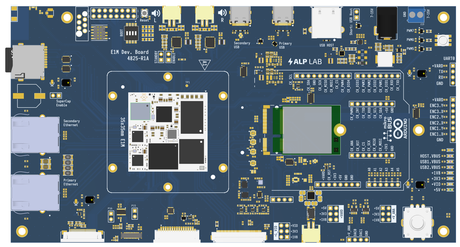
From the schematic, the EVK includes the following blocks:
- Power input and tree: barrel jack (7 to 15 V), two USB-C ports, power-good signals on each rail.
- Compute module interface: E1M 35 by 35 module footprint with USB, Ethernet, SDIO/SD, CAN, MIPI DSI/CSI, I2S, PDM, PCIe, UART, ADC/DAC, GPIO, boot pins, JTAG/SWD.
- Networking: 2 RJ45 MagJack (
ETH0,ETH1). - CAN bus:
TCAN1044Atransceiver, CAN headers,CANH/CANLjumpers (JP1 to JP4). - Storage: microSD socket plus SDIO muxing to M.2 Key E via
74LVC157. - Display: 40-pin MIPI DSI connector for
RK055HDMIPI4MA0720p panel. - Camera: RPi-compatible CSI (15-pin), standard MIPI CSI board-to-board (34-pin), parallel DVP (24-pin); camera mux
PI3WVR626, rails+1V2_CAM/+2V6_CAM, 1.8 V level shifting. Camera power rails are adjustable through feedback resistors. - Audio: two PDM microphones (
MP34DT05TR-A), twoTAS2563Class-D amps with JST speaker outputs, I2S source selection via74LVC157. - Sensors:
ICM-42670-PIMU,BMI323IMU,BMP581pressure,TCAL9538I/O expander. - Expansion: Arduino and mikroBUS mapping via
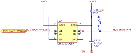
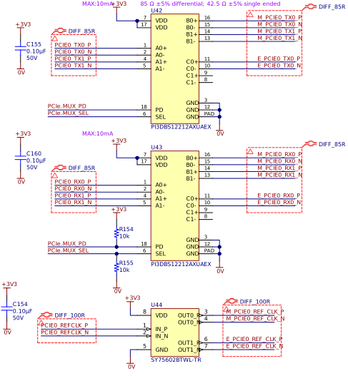
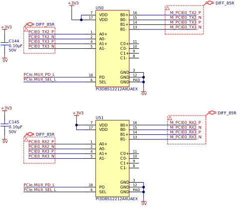
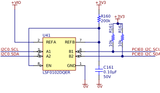
LSF0108/LSF0102level shifters; IO-voltage select header. - PCIe / M.2: M.2 Key M and Key E, PCIe mux (
PI3DBS12212A), refclk buffer (SY75602), I2C mux (TMUX121),TCAL9538for resets/interrupts. - Boot and debug: JTAG/SWD 10-pin header (
FTSH-105), reset button,BOOT0toBOOT3DIP switch, module enable header, U.FL antenna. - Current measurement: multiple
INA236monitors with shunt resistors and fixed I2C addresses; camera-rail headers P15/P16.

Power System
Power Inputs
Barrel Jack (primary)
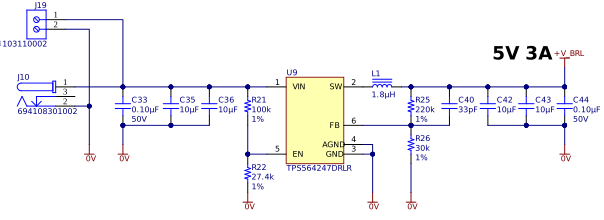
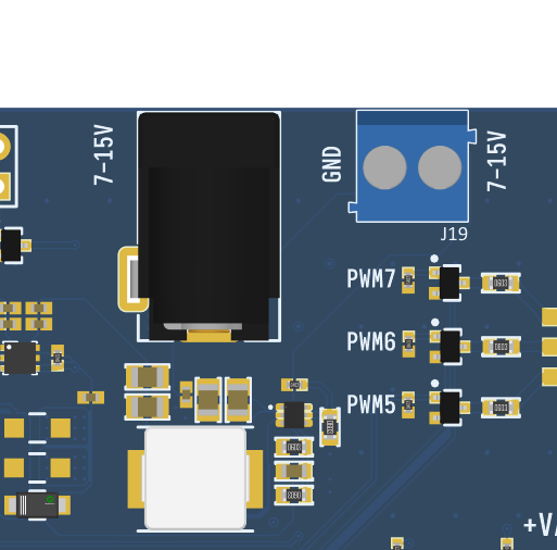
The schematic labels the barrel input 7 V to 15 V. The input rail is named +V_BRL.
USB-C Inputs
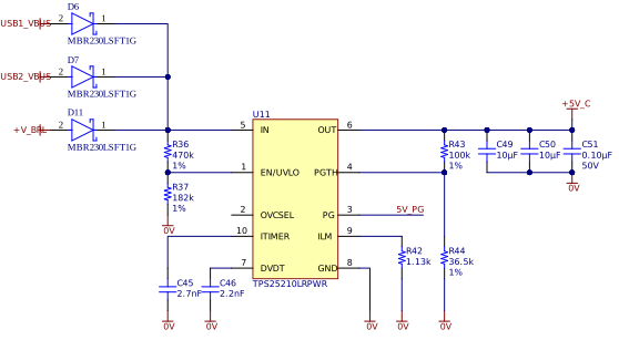
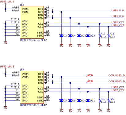
Two USB-C receptacles are present: J12 and J13. Each provides a VBUS net (USB1_VBUS / USB2_VBUS) and CC pins with 5.1 kΩ resistors.
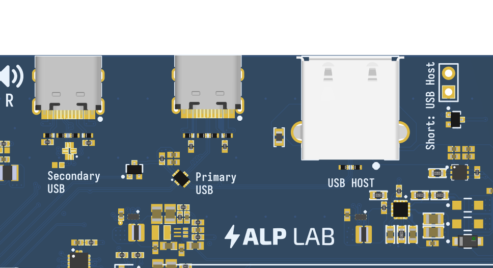
Use one primary power source at a time during early bring-up (barrel or USB-C) to avoid back-feeding paths unless you have verified the power-OR behavior on your assembled revision.
Main 5 V Generation and Protection
TPS564247buck regulator: 5 V 3 A from the barrel input path.TPS25210Lprotection and current-limit switch: produces+5Vand5V_PGpower-good.- LEDs are provided for
USB_HOST_VBUS,+3V3,+1V8,+VIO.
Secondary Rails
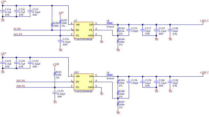
TLV62595buck regulator: generates+3V3(3V3_PG).TLV62595buck regulator: generates+1V8(1V8_PG).
SuperCap Rail
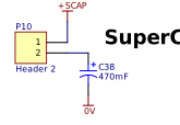
A 470 mF SuperCap (C38) sits on the +SCAP rail. The E1M interface symbol exposes pin +S_CAP and routes it in the carrier.
To enable supercap short P10.
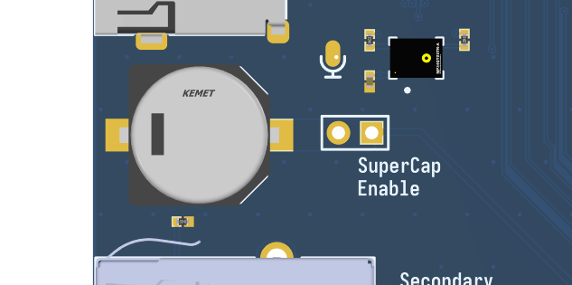
Treat the supercap rail as an energy storage node. After power-down it may remain charged. Confirm discharge behavior before handling or probing.
Boot, Reset, and Debug
Debug Connectors
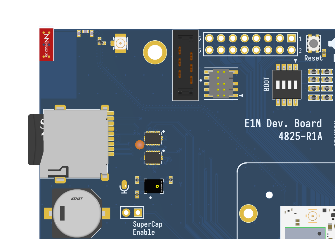
- J2: 10-pin debug header (
FTSH-105) with JTAG / SWD signals:TCK/SWDCLK,TMS/SWDIO,TDI,TDO,JTAG_RST, plus GND and+VIO. - J3: secondary debug connector labeled "Debug" (SKEDD). Not populated on the 2626-R2 (E1M-AEN) build; use
J2for SWD/JTAG. See Appendix B.
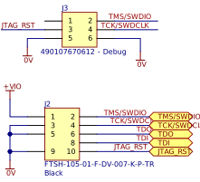
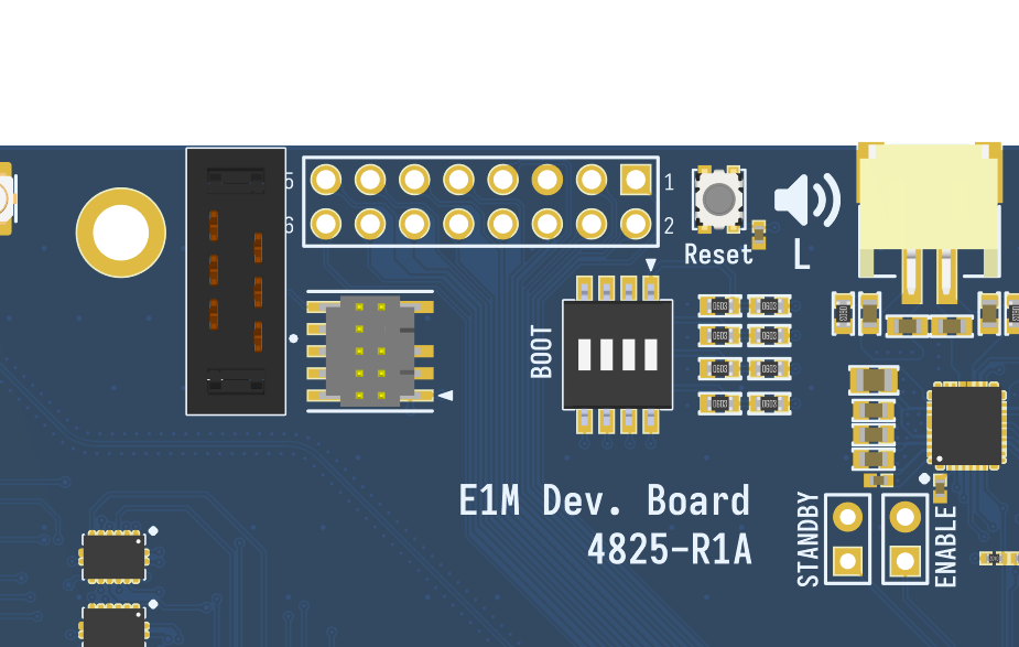
JTAG and Boot Switch
Reset
S1 is the reset switch, labeled MCU_RST. See JTAG and boot switch.
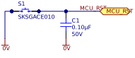
Reset pin has an internal pull-up.
Boot Mode Selection
SW1 is a DIP switch exposing BOOT0, BOOT1, BOOT2, BOOT3. See JTAG and boot switch.
Pull-up or pull-down for the boot pins must be provided inside the module (schematic annotation). The EVK only exposes the switches.
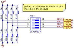
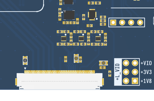
10K resistors are used as a placeholder, actual value and configuration may differ according to the specific E1M module. Refer to the datasheet.
Module Enable / Standby
- P12 header: "Short to disable module" (
MODULE_ENcontrol). - P14 header: "Short to put the module in sleep mode" (
MODULE_STBYcontrol).
See JTAG and boot switch.

Antenna
J1 is a U.FL / IPEX connector labeled ANT, with an ONE mXTEND antenna network footprint on the board.
USB Subsystem
USB-C Ports
J12 and J13 are USB-C connectors. USB2 is labeled "USB HOST" at the CC-resistor pair (R19/R20).
USB-A Host Port
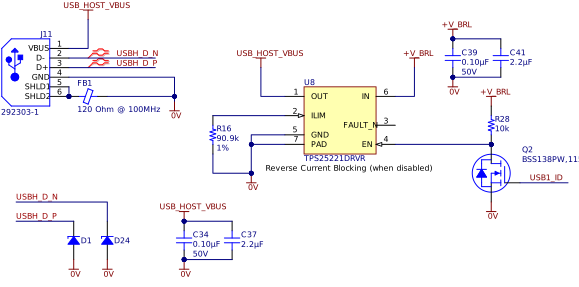
J11 is a USB-A connector. Host VBUS is gated by TPS25221 (reverse-current blocking when disabled); output net is USB_HOST_VBUS.
Data Mux and Host ID
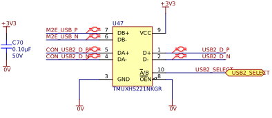
- U10
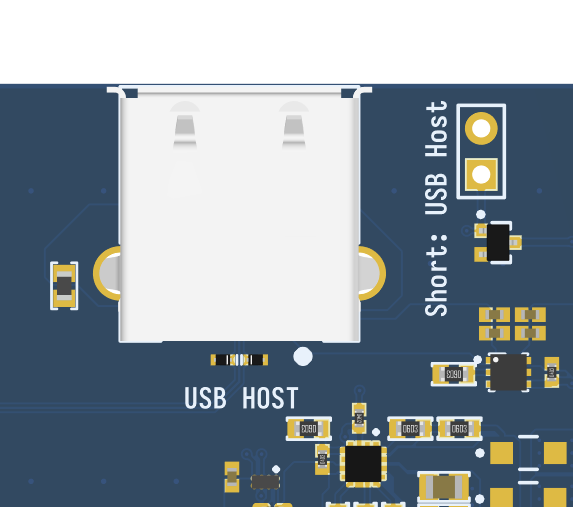
TMUXHS221: high-speed mux on the USB data lines. - P2 header labeled "Short for USB HOST" tied to
USB1_ID.
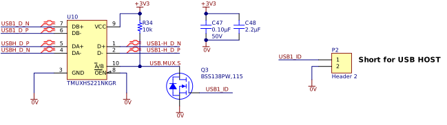
If your software expects OTG / role selection via the ID pin, use P2 to force the intended role (host).
Ethernet
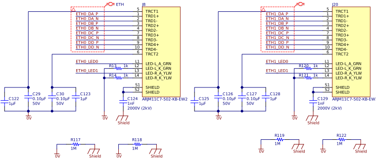
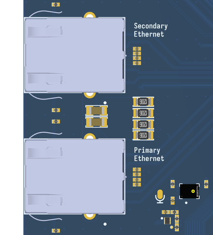
- J8:
ETH0, BelARJM11C7-502-KB-EW2integrated MagJack. - J20:
ETH1, same connector. - Differential pairs
ETHx_DA/DB/DC/DDand LED signals are routed. - Shield network includes caps and high-value resistors to chassis.
CAN Bus
Transceiver
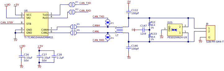
U6 TCAN1044AVDRBRQ1: signals CAN_TXD, CAN_RXD, CAN_STBY, CANH, CANL.
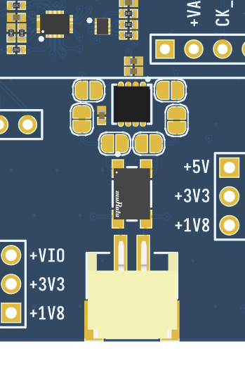
Headers and Jumpers
- JP1 to JP4:
CANH/CANLand CAN TX/RX routing jumpers. - J9: 2-pin plus shield/ground CAN pigtail connector.
Confirm whether the 120 Ω termination is populated on your BOM variant before connecting to an existing CAN network. Leaving a second terminator on a fully-terminated bus halves the effective impedance.
microSD and SDIO Muxing
microSD Socket
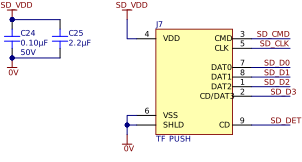
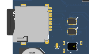
J7: push-push microSD with SD_CLK, SD_CMD, SD_D0 to SD_D3, SD_DET.
On the 2626-R2 (E1M-AEN) build the per-line ESD diodes on the SD bus (D12–D14, D27–D30, ESD9101P2T5G) are not populated. The footprints remain for builds that require board-level ESD protection on the card edge. See Appendix B.
SDIO Multiplexing
Two 74LVC157 muxes (U38 and U39) implement SDIO selection between the microSD socket and M.2 Key E SDIO. Control lines are MUX_SEL.SDIO and MUX_EN. Jumpers JP5 / JP6 sit near the M.2 SDIO reset selection.
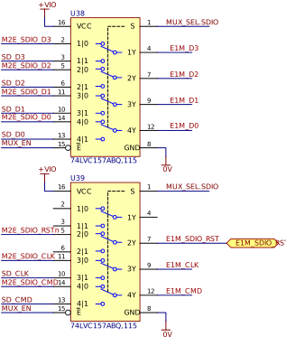
Decide whether SDIO should route to the microSD socket or to M.2 Key E (SDIO-based Wi-Fi modules) by setting the mux-control jumpers for your use case.
Display (MIPI DSI)
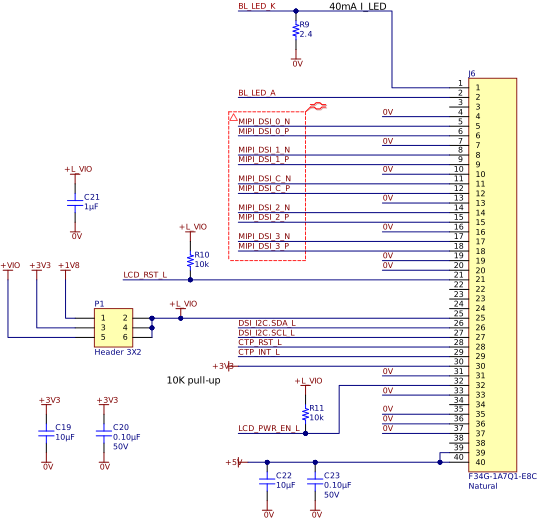
- J6: 40-pin display connector; the sheet references
RK055HDMIPI4MA0. - MIPI DSI clock + 4 data lanes (pairs) are routed.
- Backlight pins:
BL_LED_A,BL_LED_K. - Touch:
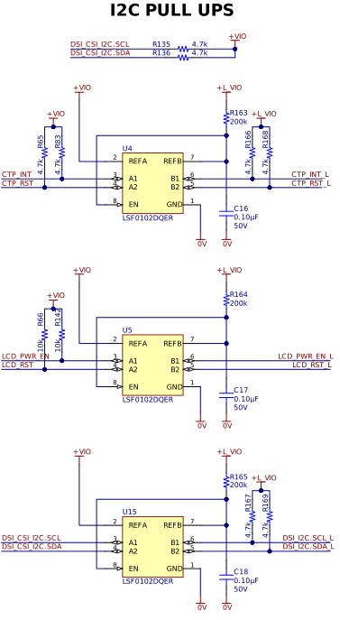
CTP_INT,CTP_RST, plus level-shifted variants and pullups. - I2C pullups are called out explicitly on the display sheet.
Camera Interfaces
RPi-Compatible CSI
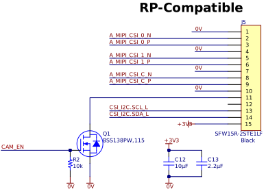
J5: 15-pin "RP-Compatible" connector; CSI CLK + two data lane pairs.
Standard MIPI Camera B2B
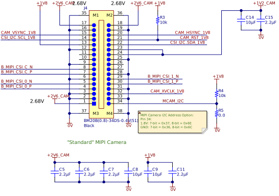
J4: 34-pin board-to-board camera connector; a power-up sequence is annotated on the sheet.
Parallel (DVP) Camera
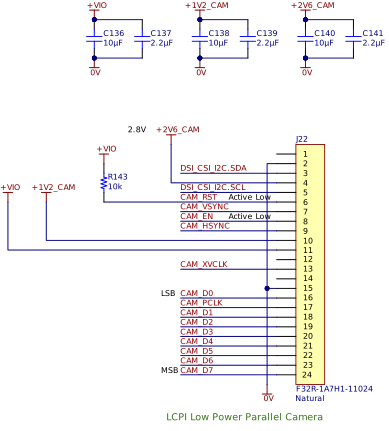
J22: 24-pin connector for a low-power parallel camera with CAM_D0 to CAM_D7, CAM_PCLK, CAM_XVCLK, CAM_HSYNC, CAM_VSYNC.
Camera Switching, Rails, and Level Shifting
- U1
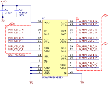
PI3WVR626: CSI lane switching between A / B ports. - Camera rails:
+1V2_CAM,+2V6_CAM.
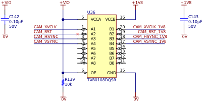
- U36
TXB0108: shifts camera control signals to 1.8 V (e.g.CAM_RST_1V8).
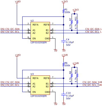
LSF0102I2C level shifters exist for CSI / DSI I2C rails.
PCIe and M.2 Expansion
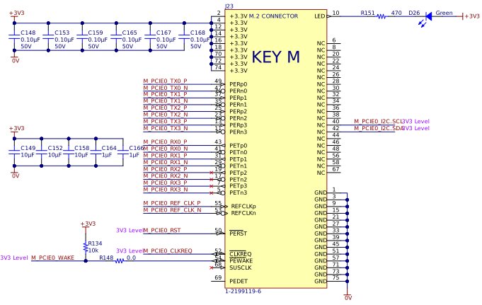
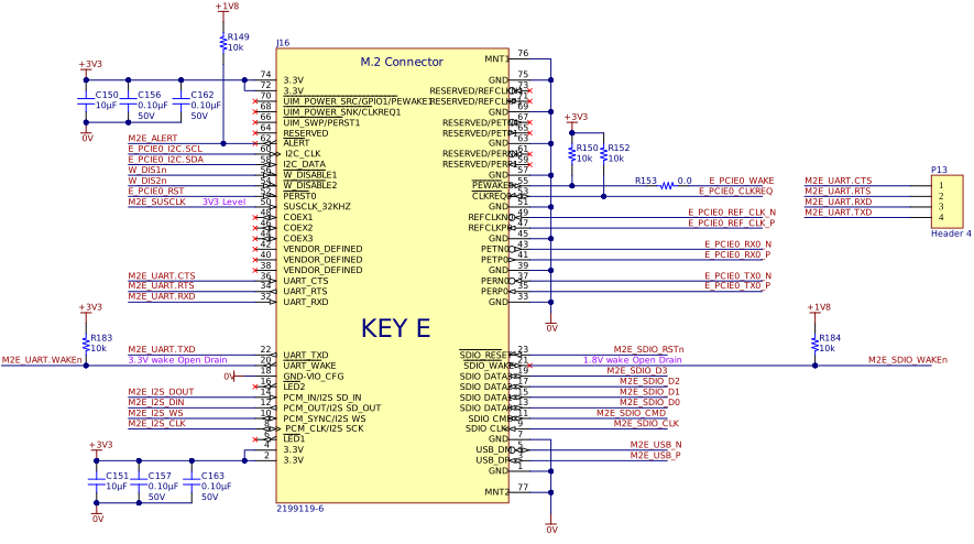
The Alif Ensemble SoCs have no PCIe, so on the 2626-R2 (E1M-AEN) assembly the M.2 card-edge connectors are not populated: J16 (Key E) and J23 (Key M), together with their PCIe AC-coupling and termination (C93–C100, R73, R74, R76, R123). The PCIe switch / buffer / I2C-mux support ICs described below remain populated for forward-compatibility with future PCIe-capable SoMs. See Appendix B for the full not-populated list.
M.2 Key M
J23: NVMe / PCIe Key M connector, multiple PCIe lanes and sidebands.
M.2 Key E
J16: Wi-Fi / BT Key E connector. Schematic notes reference standard M.2 usage: PCIe or SDIO for Wi-Fi; UART and PCM; I2C and ALERTn; NFC.
PCIe Reference Clock and Switching
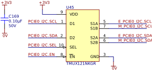
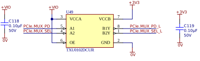
SY75602: PCIe clock buffer.PI3DBS12212A: PCIe lane mux / switch.TMUX121: PCIe I2C mux.
PCIe I/O Expander
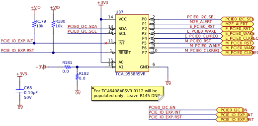
U37 TCAL9538: exposes PCIE_IO_EXP.INT and PCIE_IO_EXP.RST for the M.2 slots.
Audio
PDM Microphones
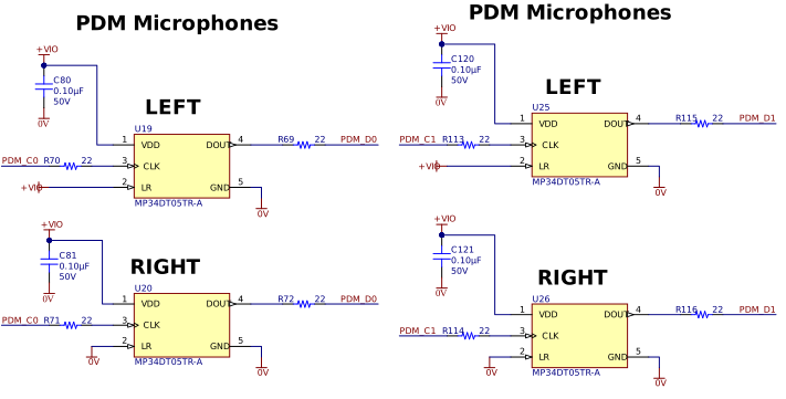
MP34DT05TR-A on MIC0 and MIC1 via the PDM_Cx / PDM_Dx clock/data nets.
Amplifiers and Speaker Outputs
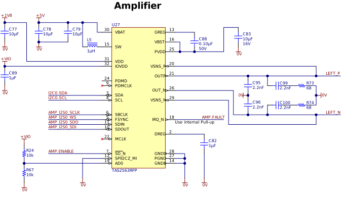
- U27, U28:
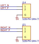
TAS2563Class-D smart-amp ICs. - Speaker outputs routed to J14 and J21 (2-pin JST connectors).
- Control:
AMP.ENABLE,AMP.FAULT.
I2S Routing
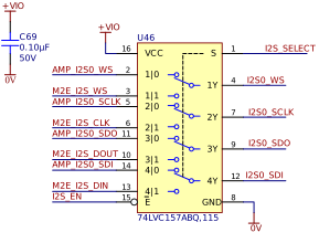
U46 74LVC157 selects the I2S source. Control nets: I2S_EN, I2S_SELECT. I2S can be sourced either from the module or from M.2 Key E (M2E_I2S nets): useful for BT audio paths.
Sensors and I/O Expansion
Sensor Devices
| Ref | Part | Role |
|---|---|---|
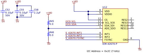
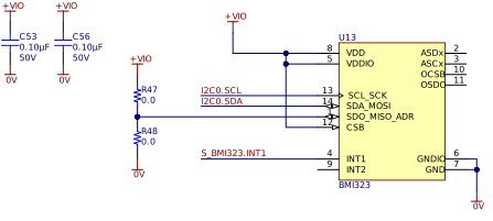
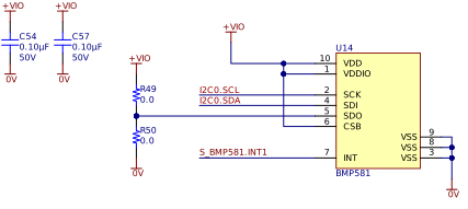
| U12 | ICM-42670-P | 6-axis IMU |
| U13 | BMI323 | 6-axis IMU |
| U14 | BMP581 | Barometric pressure |
I2C Bus and Pullups
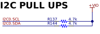
The board uses I2C0.SCL / I2C0.SDA as a shared bus for sensors and current monitors. I2C pullups are called out on the sensors sheet.
I/O Expander
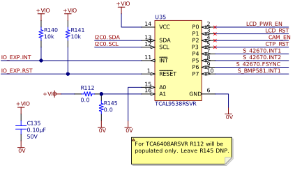
U35 TCAL9538 drives LCD_PWR_EN, LCD_RST, CTP_RST, CAM_EN, and sensor interrupts. It exposes IO_EXP.INT / IO_EXP.RST to the module.
Current Measurement (Power Profiling)
The EVK includes multiple INA236 current monitors with shunts and fixed I2C addresses. Variants on the BOM are INA236AIYBJR and INA236BIYBJR.
- Shunt examples: 50 mΩ and 20 mΩ.
- Max-current relation annotated on the sheet: Imax = 81.92 mV / R
- P15 / P16 headers relate to camera-rail measurement nodes (
+V_CAM0,+V_CAM1).
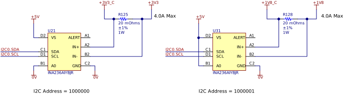
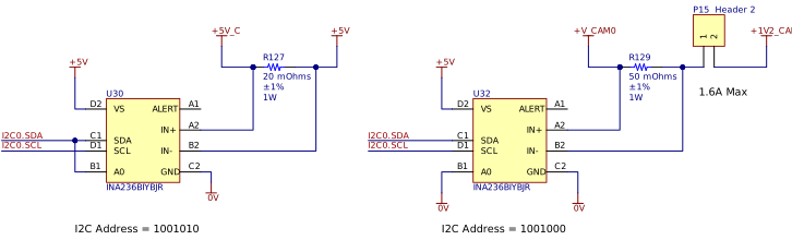
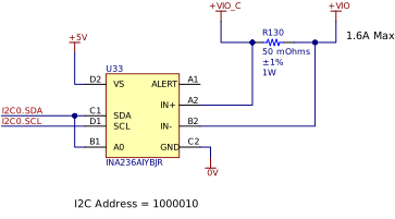
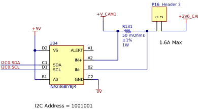
Use the INA236 monitors to log rail consumption during boot, radio activity, display usage, and camera streaming: especially useful for comparing firmware power states or module variants side-by-side.
User Interface
- Rotary encoder:
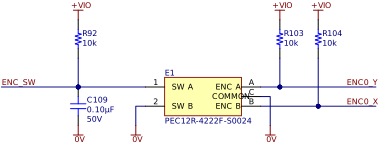
PEC12R-4222F-S0024, with switch and quadrature signals. - RGB LED:
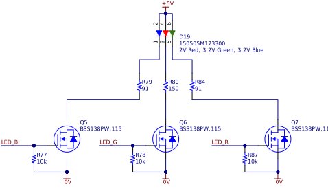
150505M173300, driven via transistors. - DAC outputs:
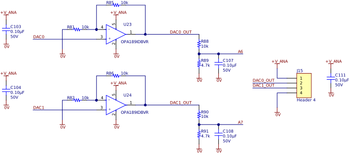
DAC0_OUT,DAC1_OUTbuffered byOPA189op-amps, routed to header J15. - Comparator signals:
CMP0,CMP1on header J18. - IO-voltage select header P17:
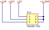
+1V8,+V_ANA,+3V3,+5V.
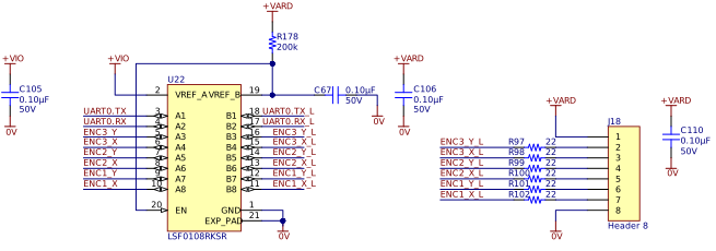
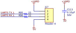
Arduino / mikroBUS Expansion
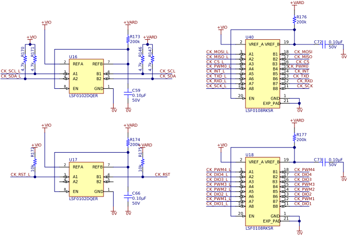
The schematic includes an "Arduino / Mikro BUS" sheet mapping signals to headers using LSF0108 and LSF0102 level shifters. The IO-voltage header selects the domain for expansion interfaces.
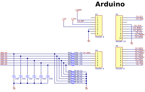
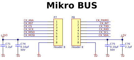
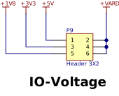
Decide your +VIO level before attaching external shields or click boards: an over-voltage on IO can damage attached peripherals.
Recommended Bring-Up Checklist
This is recommended engineering practice, not a verbatim procedure from the schematic.
- Visual inspection: check for solder bridges around the module footprint, M.2 connectors, and fine-pitch camera / display FFCs.
- Power-only test (no peripherals):
- Apply barrel input within 7 V to 15 V.
- Verify LEDs for
+3V3,+1V8,+VIO,USB_HOST_VBUS. - Probe
5V_PG,3V3_PG,1V8_PGat the indicated test points.
- Module enable: ensure
MODULE_ENis not held low (P12 is "short to disable module"). - Boot configuration: set
BOOT0toBOOT3on SW1 per your SoM firmware. - Debug access: connect to J2 (SWD/JTAG) and confirm the IO reference voltage (
+VIOon header). - Add peripherals one at a time: Ethernet, microSD, then display / camera, then M.2 modules.
Known Design Notes
From schematic annotations:
- Power sheet: Check voltage division: it boots at 13 V.
- Boot sheet: Pull-up or pull-down for the boot pins must be in the module.
These notes should be carried forward into the production release notes and errata.
Appendix A: Interface Quick Reference
Table: EVK interface summary
| Block | What's on the board |
|---|---|
| Power | Barrel 7 to 15 V, +5V / +3V3 / +1V8 / +VIO rails, PG signals, +SCAP supercap |
| USB | 2 USB-C, 1 USB-A host, HS mux, host-ID strap |
| Ethernet | 2 RJ45 MagJack (ARJM11C7-502-KB-EW2) |
| CAN | TCAN1044A transceiver plus JP1 to JP4 jumpers and J9 |
| Storage | microSD plus SDIO mux to M.2 Key E |
| Display | 40-pin MIPI-DSI (RK055HDMIPI4MA0), touch RST/INT |
| Camera | RPi CSI 15-pin, MIPI B2B 34-pin, DVP 24-pin, camera mux plus rails |
| Audio | 2 PDM mic, 2 TAS2563, I2S mux, JST speaker headers |
| Sensors | ICM-42670-P, BMI323, BMP581, TCAL9538 I/O expander |
| PCIe/M.2 | Key M plus Key E, PCIe lane mux, refclk buffer, I2C mux |
| Debug | J2 SWD/JTAG, reset, BOOT0 to BOOT3, P12/P14, U.FL antenna |
| Expansion | Arduino plus mikroBUS, IO-voltage select |
| Profiling | INA236 monitors with shunts and fixed I2C addresses |
Appendix B: Assembly Variant — E1M-AEN (Alif) Build
The E1M EVK carrier is laid out to the full E1M standard (superset) pinout. When assembled for an E1M-AEN (Alif Ensemble) module, the features that the SoM does not expose are left unpopulated. The list below is taken from the 2626-R2 BOM (35 not-populated designators); footprints remain on the PCB so the same carrier can be rebuilt for other E1M variants.
Table: Not-populated components — 2626-R2 (E1M-AEN) build
| Designator(s) | Function | Reason not fitted |
|---|---|---|
J16, J23 | M.2 Key E / Key M card-edge connectors | Alif Ensemble has no PCIe; the M.2 slots are unused. |
C93–C100, R73, R74, R76, R123 | PCIe lane / ref-clock AC-coupling and termination | Support the unfitted M.2 slots. |
D12–D14, D27–D30 | microSD line ESD diodes (ESD9101P2T5G) | Optional card-edge ESD protection; omitted on this build. |
J3 | Secondary "Debug" connector (SKEDD) | Primary SWD/JTAG is J2; the secondary header is unused. |
L4, R111 | On-board antenna feed (22 nH inductor, 0 Ω jumper) | AEN uses the module RF path / J1 U.FL; the on-board feed is open. |
R5, R10, R11, R24, R46, R47, R50, R75, R145, R181, R200 | Configuration jumpers and pull resistors | Build-time options left open on the AEN assembly. |
Release History
Table: Release History
| Revision | Changes | Date |
|---|---|---|
| 0.1 | Initial draft | April - 2026 |
| 0.2 | Documented the 2626-R2 assembly variant: not-populated components for the E1M-AEN (Alif) build (M.2 Key E/M connectors and PCIe AC-coupling, microSD ESD diodes, secondary debug J3, antenna feed, option jumpers). Added Appendix B and inline notes. | June - 2026 |