E1M Specification
- Designation: E1M-STD-1.0
- Edition: 1.0
- Revision: 1.5
- Date: 2026-10-19
- Status: Released
- Publisher: Alp Lab AB
Abstract
E1M (Edge-1 AI Module) is an open standard for solder-down LGA system-on-modules in two form factors: E1M, 35 × 35 mm with 312 pads, and E1M-X, 45 × 65 mm with 496 pads. The specification defines the footprint, the mechanical envelope, the pinout and signal assignment, the electrical and power rules, the alternative-function policy, and conformance for SoMs and carrier boards. The pinout is published as machine-readable Loom v1 JSON. The standard and its pinout are open; the individual modules built on it are separate products.
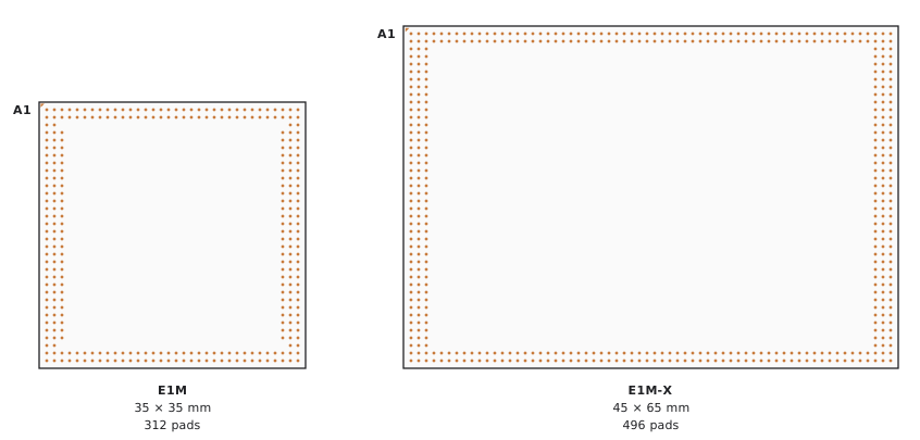
E1M and E1M-X form factors at the same scale (top view, pad A1 top left; E1M-X 65 mm across, 45 mm down; pad ring from the pinout JSON)
Reference implementation: pinout/v1.json (E1M, 35 × 35 mm) and pinout/x-v1.json (E1M-X, 45 × 65 mm) in the e1m-spec repository, validated by pinout/schema/loom-v1.schema.json.
Foreword
This specification is published by Alp Lab AB as an open standard for small-form-factor, AI-capable, machine-processable System-on-Module (SoM) products.
The standard fixes the carrier-board pinout, mechanical envelope, and electrical interface of two module form factors — E1M (35 × 35 mm) and E1M-X (45 × 65 mm) — so that a single carrier board can host modules built around different MCU, MPU, AI-accelerator, and memory silicon, provided each module conforms to this specification.
Per-SoM design files (schematics, PCB layout, manufacturing data, firmware) are not part of this specification. Each conformant SoM publishes a per-SoM manifest declaring the routed subset of E1M pads and the silicon behind those pads (see Annex C).
The pinout JSON files in this repository are mechanically generated from the Altium pin-list exports kept under source/. The CI workflow re-runs the generator on every push and rejects any commit that drifts from the source.
This edition (1.0) is the first public release. Subsequent revisions follow the versioning rules in §1.5.
Introduction
E1M defines the universe of physical pads on a 35 × 35 mm or 45 × 65 mm LGA SoM and which peripheral signals each pad may carry. The standard is intentionally silicon-agnostic: it specifies pad-to-signal assignments at the default-function level, and adds GPIO as a universal secondary on every digital pad. Anything beyond the default plus GPIO secondary — such as silicon-specific alternate functions — is declared by the per-SoM manifest and falls outside E1M conformance.
The two form factors share the same family of signal classes; E1M-X adds higher pad density to expose additional controllers (more PCIe ports, more MIPI CSI lanes, parallel LCD, etc.) than fits on E1M.
1 Scope
1.1 What this specification covers
This specification defines, for the E1M and E1M-X form factors:
- The mechanical envelope (outline, height, mounting on the carrier, component placement areas).
- The electrical interface (power input, voltage rails, reset, boot strap, electrical characteristics).
- The complete pinout (every pad's coordinate, default function, and the signal classes it may carry under the alternative-function policy in §8).
- The conformance criteria for SoMs and carrier boards (§9).
- The pinout JSON format (Loom v1) used to consume the standard programmatically (Annex B).
1.2 What this specification does not cover
- The internal design of any SoM (silicon, supporting components, software). These are SoM-vendor-specific and live outside this repository.
- Per-SoM peripheral mappings beyond the default and GPIO secondary functions. These live in per-SoM manifests (Annex C).
- Carrier-board reference designs.
- Marketing claims or feature endorsements.
1.3 Audience
- SoM designers producing E1M-conformant modules.
- Carrier-board designers producing baseboards, breakout boards, or end products that mount an E1M SoM.
- Tooling authors producing EDA libraries, schematic generators, or build systems that consume the pinout JSON.
1.4 Conventions
The keywords MUST, MUST NOT, REQUIRED, SHALL, SHALL NOT, SHOULD, SHOULD NOT, RECOMMENDED, MAY, and OPTIONAL in this document are to be interpreted as described in RFC 2119.
Throughout this document:
- Pad identifiers (e.g.
A1,K63,AQ15) follow the BGA-style convention: row letter(s) followed by column number, in the coordinate space of the named form factor (§4.3, §7.1). - Pin names in monospace (e.g.
I2C0_SCL) match thesilkscreenfield of the corresponding pad in the pinout JSON. - A value of TBD indicates a parameter intentionally not yet specified in this revision.
1.5 Versioning
The form-factor uses major.minor versioning:
- A major bump is required for any backwards-incompatible pad change — for example, removing a pad, narrowing the SignalKind set a pad may carry, or shifting a pad's coordinate.
- A minor bump is permitted for additions only — for example, populating a previously-reserved pad or adding an alt-function entry to an existing pad.
Released editions are tagged v<major>.<minor> in this repository (e.g. v1.0).
2 Normative references
The following documents are referenced normatively. Where a dated reference is given, only that revision applies. Where an undated reference is given, the latest revision (including any amendments) applies.
| Reference | Title |
|---|---|
| RFC 2119 | Key words for use in RFCs to Indicate Requirement Levels, S. Bradner, March 1997. |
| Loom format v1 | pinout/schema/loom-v1.schema.json in the e1m-spec repository. |
3 Terms, definitions, and abbreviations
3.1 Terms and definitions
- carrier board: Host PCB that mates with an E1M SoM via the LGA pad pattern defined in §5 and §7.
- conformant: Satisfying every SHALL clause in §9 for the applicable role (SoM or carrier board).
- default function: The single primary signal that an E1M pad SHALL carry on every conformant SoM that exposes that pad. Recorded in the
defaultfield of the pad's JSON entry and in the Pin name column of §7.3. - form factor: One of the two mechanical envelopes defined in §4.
- module / SoM (System-on-Module): Self-contained compute LGA module conforming to this specification.
- pad: Physical contact on the SoM's LGA package, identified by a BGA-style coordinate.
- per-SoM manifest: A separate, vendor-supplied document that declares which E1M pads a particular SoM routes and the silicon behind them (Annex C).
3.2 Abbreviations
| Term | Meaning |
|---|---|
| ADC | Analogue-to-digital converter |
| BGA | Ball-grid array (used here for the pad-numbering convention) |
| CAN | Controller area network |
| CSI | (MIPI) Camera Serial Interface |
| DAC | Digital-to-analogue converter |
| DSI | (MIPI) Display Serial Interface |
| ENC | Quadrature encoder |
| GPIO | General-purpose input / output |
| I2C, I3C | Inter-integrated circuit, version 2 / version 3 |
| I2S | Inter-IC sound |
| JTAG | Joint Test Action Group test interface |
| LCD | Liquid-crystal display (parallel RGB) |
| LGA | Land-grid array |
| LDO | Low-dropout regulator |
| NC | Not connected |
| PCIe | Peripheral Component Interconnect Express |
| PDM | Pulse-density modulation (microphone) |
| PMIC | Power-management IC |
| PWM | Pulse-width modulation |
| RSVD | Reserved for future use |
| SDIO | Secure-digital input/output |
| SoM | System-on-Module |
| SPI | Serial peripheral interface |
| SWD | (ARM) Serial-wire debug |
| TPM | Trusted Platform Module |
| UART | Universal asynchronous receiver-transmitter |
| WS | Word select (I2S frame strobe) |
4 Form factors
4.1 E1M ("Normal")
| Attribute | Value |
|---|---|
| Outline | 35 × 35 mm, ±0.1 mm (TBD) |
| Pad pattern | LGA |
| Pad count | 312 |
| Coordinate space | Rows A–AH (top to bottom), columns 1–34 (left to right), top view |
| Reference SoMs | E1M-AEN family — seven SKUs E1M-AEN301/401/501/601/701/801/803 (Alif Semiconductor Ensemble E3– E8). |
4.2 E1M-X ("Extended")
| Attribute | Value |
|---|---|
| Outline | 45 × 65 mm, ±0.1 mm (TBD) |
| Pad pattern | LGA |
| Pad count | 496 |
| Coordinate space | Rows A–AR (top to bottom, along the 45 mm side), columns 1–64 (left to right, along the 65 mm side), top view; the outline is 65 mm across and 45 mm down |
| Reference SoMs | E1M-X V2N family — E1M-V2N101/E1M-V2N102/E1M-V2N103. E1M-X V2N-M1 family — E1M-V2M101/E1M-V2M102/E1M-V2M103 (Renesas RZ/V2N + DRP-AI3 + optional DeepX M1). |
4.3 Coordinate system
Each form factor uses an independent coordinate space. Pad A1 on E1M is not the same physical position as pad A1 on E1M-X. In both, in the top view (component side up), the pad letters name the rows, running top to bottom, and the pad numbers name the columns, running left to right; pad A1 is the top-left corner pad, 1.0 mm from the left and top edges, next to the pin-1 fiducial. A2 is directly right of A1 and B1 is directly below A1. The pad band is two pads deep along the top and bottom edges (rows A, B and the last two rows) and three pads deep along the left and right edges (columns 1–3 and the last three columns). In this frame the E1M-X outline is 65 mm across (columns 1–64) and 45 mm down (rows A–AR). The outline_mm field of pinout/x-v1.json (w = 45, h = 65) records the outline size; it does not set the drawing orientation. SoM manifests reference pads by (form-factor id, coordinate). The form-factor identifier E1M or E1M-X is recorded in the top-level id field of the corresponding pinout JSON.
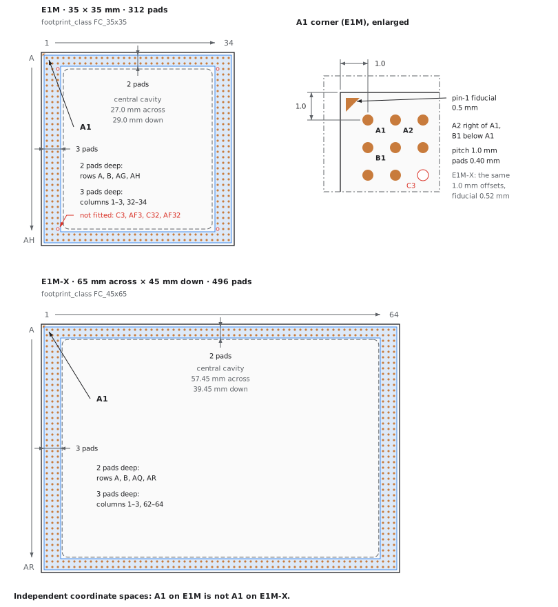
(informative): E1M and E1M-X coordinate frames at the same scale, top view. Row letters run top to bottom and column numbers left to right; the shaded pad band is two pads deep at the top and bottom edges and three pads deep at the left and right edges. Pad A1 sits 1.0 mm from the left and top edges, next to the pin-1 fiducial; A2 is right of A1, B1 below it. E1M-X is drawn landscape, 65 mm across and 45 mm down. The two coordinate spaces are independent.
5 Mechanical requirements
5.1 Footprint
5.1.1 E1M (35 × 35 mm)
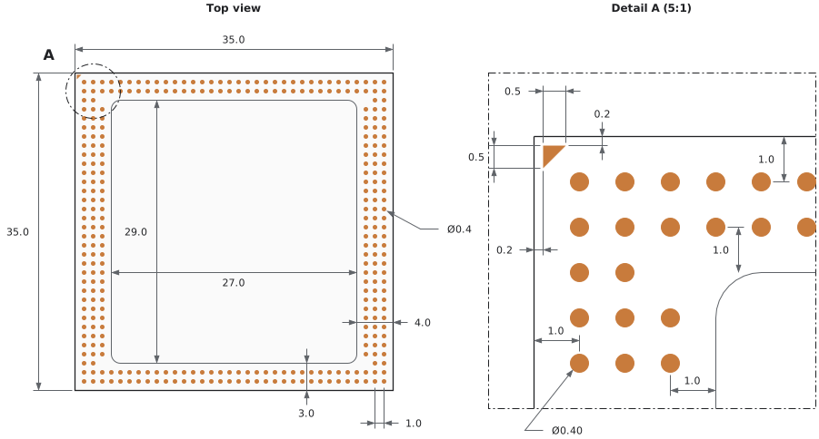
E1M footprint mechanical drawing
The E1M signal pads SHALL lie on a 1.0 mm pitch grid and SHALL be 0.40 mm diameter round copper pads. The recommended carrier land pattern is given in §5.1.3 (informative).
Dimension tolerances other than the outline, and a carrier-board footprint library, are not specified in this revision.
5.1.2 E1M-X (45 × 65 mm)
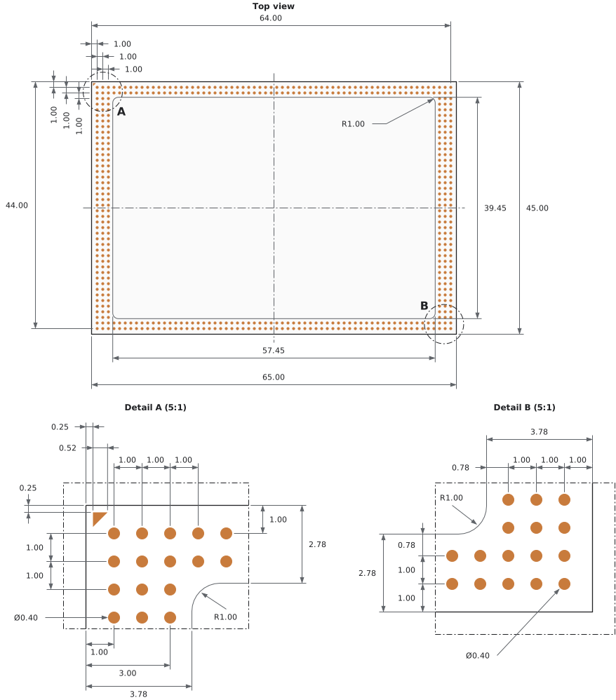
E1M-X footprint mechanical drawing
Dimension callouts and a carrier-board footprint library for E1M-X are not specified in this revision.
5.1.3 Recommended carrier land pattern (informative)
The land pattern below is recommended for the carrier board of both form factors. Its pad, solder-mask and stencil values are the carrier land pattern published for E1M-AEN (DS-AEN-001) (E1M-AEN only); the pad pitch and the copper pad diameter are those of §5.1.1 and of the E1M-X footprint drawing (§5.1.2). The courtyard is 2.0 mm clearance around the module outline on every side. For mounting option (b) of §5.2 the through-cutout is part of the carrier land pattern; its size, position and corner radius are normative (§5.2).
| Parameter | Value | Provenance |
|---|---|---|
| Land-pattern density | IPC-7351 nominal | (E1M-AEN only) |
| Pad pitch (signal grid) | 1.0 mm | §5.1.1, §5.1.2 |
| Copper pad | round, NSMD, 0.40 mm diameter | §5.1.1, §5.1.2; NSMD: (E1M-AEN only) |
| Solder-mask opening | 0.50 mm diameter | (E1M-AEN only) |
| Stencil aperture | 1:1, 0.40 mm diameter | (E1M-AEN only) |
| Stencil thickness | 0.08 mm | (E1M-AEN only) |
| Courtyard | module outline + 2.0 mm on every side: E1M 39.0 × 39.0 mm; E1M-X 69.0 mm across × 49.0 mm down | §5.1.3 |
| Through-cutout, mounting option (b) only | central-cavity size and position, R1.00 corners: E1M 27.0 mm across × 29.0 mm down, 4.0 mm from the left and 3.0 mm from the top edge of the module outline; E1M-X 57.45 mm across × 39.45 mm down, 3.775 mm from the left and 2.775 mm from the top edge | §5.2 (normative) |
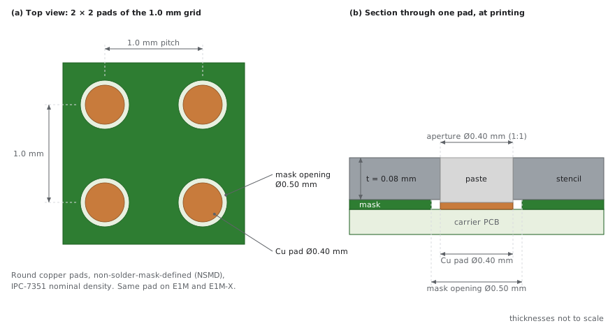
(informative): Recommended carrier land pattern, pad detail. (a) Top view of four pads of the 1.0 mm grid with the 0.40 mm copper pads inside the 0.50 mm solder-mask openings; (b) section through one pad with the 1:1 stencil aperture and the 0.08 mm stencil, thicknesses not to scale.
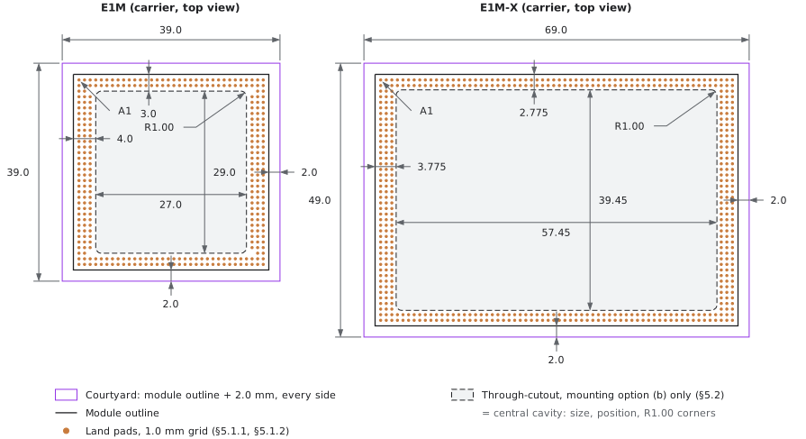
(informative): Recommended carrier land pattern, E1M (left) and E1M-X (right), carrier top view with A1 top left: module outline, 2.0 mm courtyard (E1M 39.0 × 39.0 mm, E1M-X 69.0 mm across × 49.0 mm down), land pads, and the through-cutout of mounting option (b) (dashed; §5.2) at the central-cavity size and position with R1.00 corners. A carrier that uses mounting option (a) has no cutout.
Pad position and size tolerances are not specified in this revision (§5.1.1).
5.2 Mounting
A SoM SHALL NOT be placed directly on the carrier board. One of the following two mounting options SHALL be used:
- Option (a), spacer PCB. A spacer PCB SHALL be placed between the SoM and the carrier board, soldered on both faces: the SoM's LGA pads SHALL be soldered to the spacer PCB and the spacer PCB SHALL be soldered to the carrier board (§5.2.1). The carrier SHALL keep the area under the SoM's central cavity clear: no carrier component SHALL lie inside the cavity outline given below, with or without a spacer PCB.
- Option (b), carrier cutout. The carrier board SHALL have a through-cutout the size of the SoM's central cavity, at the cavity position, with R1.00 corners (§5.2.2). In the top view of §4.3, the cutout is:
- E1M: 27.0 mm across × 29.0 mm down, its left edge 4.0 mm from the left edge and its top edge 3.0 mm from the top edge of the module outline (§5.1.1);
- E1M-X: 57.45 mm across × 39.45 mm down, its left edge 3.775 mm from the left edge and its top edge 2.775 mm from the top edge of the module outline (§5.1.2).
A SoM carries components on its bottom side, under its central cavity, inside the LGA pad band (§5.3). Placed directly on the carrier, these components would meet the carrier surface. The spacer PCB of option (a) raises the SoM above the carrier; the cutout of option (b) gives the bottom-side components room through the carrier board.
5.2.1 Option (a): spacer PCB
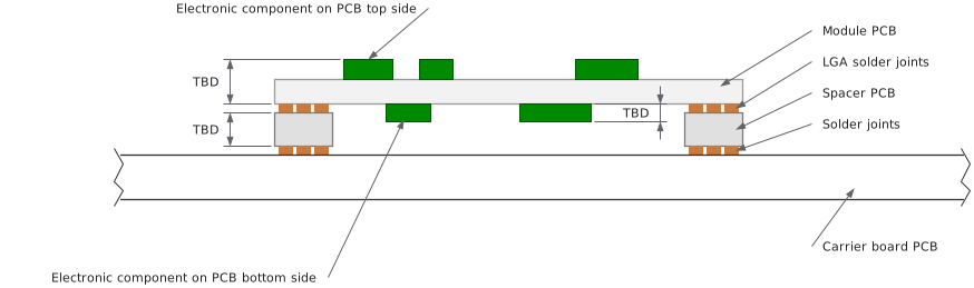
Module on a spacer PCB (mounting option (a))
The module is soldered to the spacer PCB and the spacer PCB is soldered to the carrier board, so each of the two faces of the spacer PCB carries a solder joint. The carrier SHALL have no components inside the cavity outline of §5.2 (E1M 27.0 mm across × 29.0 mm down, 4.0 mm from the left and 3.0 mm from the top edge of the module outline; E1M-X 57.45 mm across × 39.45 mm down, 3.775 mm from the left and 2.775 mm from the top edge; R1.00 corners). The spacer-PCB thickness, the maximum module thickness and the maximum component height on the SoM bottom side are not specified in this revision.
5.2.2 Option (b): carrier cutout
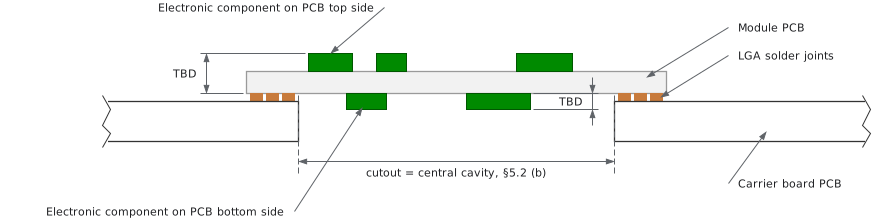
Module over a carrier cutout (mounting option (b))
The maximum module thickness, the maximum component height on the SoM bottom side and the LGA pad stand-off are not specified in this revision.
5.3 Component placement areas
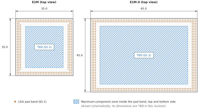
Component placement areas — E1M and E1M-X
On the SoM bottom side the zone lies inside the central cavity, which the spacer PCB (option (a)) or the carrier cutout (option (b)) of §5.2 keeps clear of the carrier surface; under either option the carrier has no components inside the cavity outline. On the carrier, the SoM occupies the courtyard of §5.1.3.
Where present, EMI shielding SHALL fit within the module height envelope (§5.2).
Numeric keepout dimensions for the placement zones are not specified in this revision.
5.4 Soldering
E1M and E1M-X SHALL be solderable to the carrier board using LGA-class reflow soldering. Where a particular SoM is also compatible with BGA-class reflow profiles, the per-SoM manifest MAY declare this.
5.4.1 Recommended reflow profile (informative)
The profile below is informative. Its values are those measured for E1M-AEN in a JTR1000 convection reflow oven with ALPHA OM338 solder paste (SAC, Pb-free); each measured value is given as the range measured on the module. The profile phases follow IPC/JEDEC J-STD-020. The process windows are those of the profiler report for this run. A recommended reflow profile for the other reference SoMs is not specified in this revision.
| Parameter | Measured, E1M-AEN | Process window (informative) |
|---|---|---|
| Reflow oven | JTR1000 | — |
| Solder paste | ALPHA OM338 (SAC, Pb-free) | — |
| Preheat, 30–150 °C | 116.5–122.0 s | 60–160 s |
| Soak, 150–217 °C | 70.5–73.5 s | 60–120 s |
| Time at or above 220 °C | 56.5–60.0 s | 45–90 s |
| Cooling slope, from 220 °C | −1.53 to −1.66 °C/s | −4 to −0.5 °C/s |
| Peak temperature | 240.9–244.3 °C | 230–250 °C |
| Profile reference | IPC/JEDEC J-STD-020 | — |
The solder-paste liquidus is 217 °C; the time-above-reflow values are measured at 220 °C, as in the profiler report. Figure 10 shows one measured curve of this run, with its own values (preheat 116.5 s, soak 71.5 s, at or above 220 °C 60.0 s, cooling −1.53 °C/s, peak 242.9 °C), which lie within the measured ranges of the table.
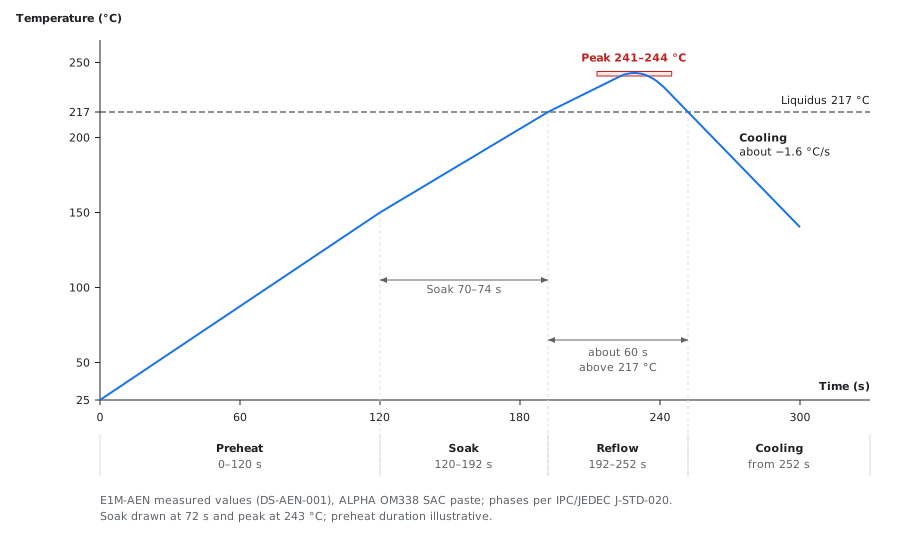
(informative): Measured reflow profile of the E1M-AEN (JTR1000 oven, ALPHA OM338), with the 150 °C, 217 °C (liquidus) and 220 °C levels and the phase spans.
5.5 Packaging
Packaging requirements are not specified in this revision.
6 Electrical requirements
6.1 Power architecture
Conformant SoMs SHALL generate every internal supply rail on board from a single externally-supplied 5 V input on the VDD_5V_IN pads (silkscreen VDD on E1M; see §7.3.1). On-module power management SHALL be performed by an I2C-controlled PMIC.
A SoM SHALL expose a regulated 1.8 V I/O reference rail on the VIO_OUT pads, sized to power any I/O level-shifting on the carrier board (§6.1.2).
A SoM SHALL include all decoupling capacitors required for correct on-module operation. Carrier-board designers SHOULD add additional decoupling capacitors close to high-current loads on the carrier side.
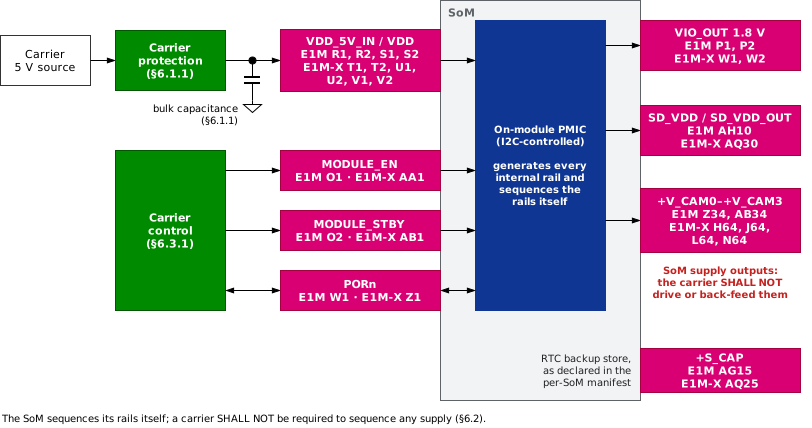
(informative): Power architecture. The carrier feeds the VDD_5V_IN pads through its protection and bulk capacitance (§6.1.1); the on-module PMIC generates and sequences every internal rail; VIO_OUT, SD_VDD_OUT / SD_VDD and +V_CAM0–+V_CAM3 are SoM supply outputs.
Where a value in §6 is marked (E1M-AEN only), it is confirmed by the E1M-AEN documentation (DS-AEN-001 / HG-AEN-001, hw_rev R3) and is still TBD in the E1M-X V2N and V2N-M1 documentation. Where it is marked (E1M-X V2N / V2N-M1 only), the reverse applies. Such values bind every SoM and every carrier until a later revision states otherwise.
6.1.1 5 V supply input
The clauses below define the 5 V window for a carrier that hosts any conformant SoM. The window is the strictest combination of the windows of the reference SoMs (Annex A).
- Operating window. The carrier SHALL hold the voltage at the
VDD_5V_INpads between 4.75 V and 5.25 V, measured at the pads, at every load up to the peak input current the SoM declares. - Absolute maximum. The carrier SHALL keep the voltage at the
VDD_5V_INpads at or below 5.5 V at all times, including transients, load release and hot-plug overshoot. A transient-voltage suppressor alone does not meet this clause, because the clamp voltage of a 5 V TVS is well above 5.5 V; an over-voltage cut-off or clamp (for example an eFuse or load switch with over-voltage protection) is needed ahead of the pads. - Ramp. The rise of
VDD_5V_INfrom 0 V to 4.75 V SHALL be monotonic and SHALL complete within 40 ms (E1M-AEN only). - Pads. The carrier SHALL connect every
VDD_5V_INpad (E1M:R1,R2,S1,S2; E1M-X:T1,T2,U1,U2,V1,V2) to the 5 V supply through a low-impedance path, and SHALL NOT connect any other supply to them. - Current. The carrier 5 V source SHALL be sized for the peak input current the SoM declares, not for its average current, plus every carrier load that shares the source.
- Input protection. A SoM is not required to include input protection. The carrier SHALL provide the over-voltage protection that clause 2 needs and, where the 5 V input connector can be mis-wired, reverse-polarity protection.
- Hold-up capacitance. The carrier SHALL place, next to the
VDD_5V_INpads, at least the bulk capacitance the SoM declares. - Source OR-ing. Where the carrier can feed
VDD_5V_INfrom more than one source, it SHALL NOT back-feed an inactive source (use a unidirectional eFuse or an ideal-diode controller). The voltage drop of the OR-ing element SHALL still leave at least 4.75 V at the pads (clause 1). - SoM side. A conformant SoM SHALL operate across 4.75–5.25 V at its
VDD_5V_INpads, SHALL withstand 5.5 V without damage, and SHALL start correctly from any monotonic ramp that reaches 4.75 V within 40 ms (ramp value: E1M-AEN only). The SoM SHALL declare in its manifest its operating range, absolute maximum, peak input current, on-module input capacitance and the minimum carrier bulk capacitance.
A carrier that declares (§8.4, §9.2) that it hosts only SoMs whose manifests declare a wider window MAY use that wider window.
Figure 12 shows a carrier input chain that meets these clauses.
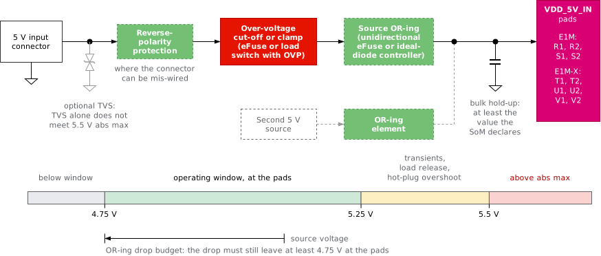
(informative): Carrier 5 V input chain (§6.1.1) and the voltage window at the VDD_5V_IN pads. Dashed blocks are needed only where the clauses above call for them.
| Parameter | E1M-AEN (DS-AEN-001, hw_rev R3) | E1M-X V2N / V2N-M1 (DS-V2N-001, DS-V2N-M1-001) |
|---|---|---|
| Operating range (min / typ / max) | 4.75 / 5.0 / 5.25 V | 4.5 / 5.0 / 5.5 V (the HG documents recommend ±5 %) |
| Absolute maximum | 5.5 V | 6.0 V |
| Ramp | monotonic, 0 V to 4.75 V within 40 ms | not specified |
| Peak input current | 834 mA (E1M-AEN801, calculated) | TBD; carrier 5 V source ≥ 5 A peak recommended |
| On-module input capacitance | about 50 µF | not specified |
| Carrier bulk capacitance | ≥ 50 µF effective per A of total VDD_5V_IN load | ≥ 10 µF + 100 nF |
6.1.2 VIO_OUT
- Level.
VIO_OUTSHALL be 1.8 V nominal, with a tolerance of ±5 % (tolerance: E1M-X V2N / V2N-M1 only; E1M-AEN TBD). No otherVIO_OUTlevel is defined in this revision. - Direction.
VIO_OUTis a SoM output. The carrier SHALL NOT driveVIO_OUT, connect it to any other rail, or connect any source that can raise it above the SoM's own level. - Permitted uses. The carrier SHALL use
VIO_OUTonly (a) as the SoM-side supply or reference (VCCA / VREF) of carrier level translators and as the pull-up rail for signals into the SoM's 1.8 V pads, (b) as a module-on indication, or (c) as the enable input of a carrier load switch that generates a carrier 1.8 V rail that follows the SoM. Any other carrier load that must follow the SoM SHALL be supplied from such a switched rail (use c). - Load limits. The SoM SHALL declare in its manifest the maximum load current and the maximum external capacitance on
VIO_OUT. A carrier that hosts any SoM SHALL keep the totalVIO_OUTload at or below 100 mA, SHALL draw no more than 50 mA during the first 2 ms afterVIO_OUTrises, and SHALL keep the total capacitance onVIO_OUTat or below 2.5 µF (E1M-AEN only; E1M-X V2N / V2N-M1: TBD). Excess capacitance can stop the SoM's 1.8 V rail from starting. - Translator power-off behaviour. Every level translator referenced to
VIO_OUTSHALL keep both of its ports high-impedance while itsVIO_OUT-side supply is off (Ioff or partial-power-down specified). Some pass-gate translators conduct with VCCA at 0 V and do not meet this clause. - Sensing. A carrier that monitors
VIO_OUTSHALL do so through a high-impedance input whose own supply is on whenever the SoM can be powered, so that the monitor cannot back-power an unpowered host.
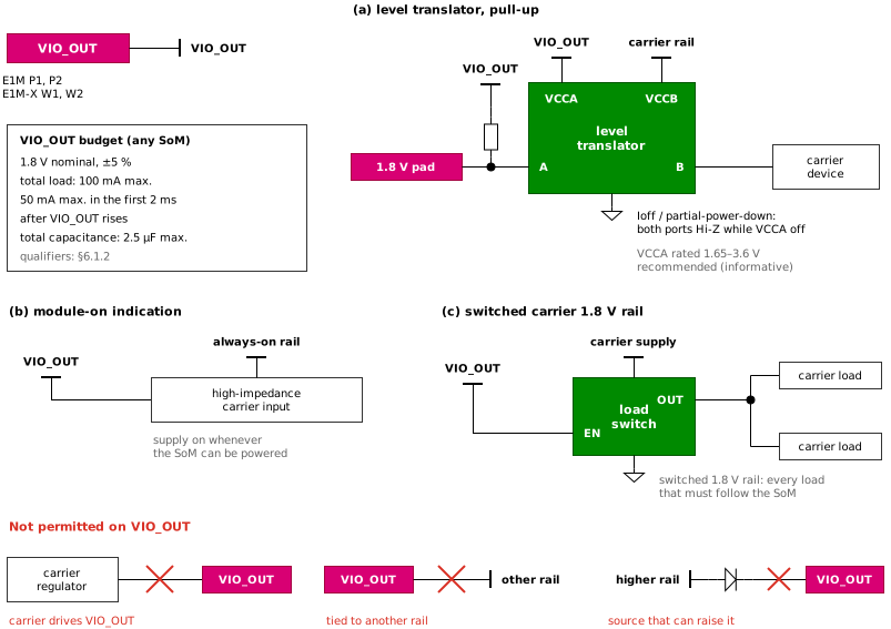
(informative): Permitted carrier uses of VIO_OUT (clause 3): (a) supply of level translators and pull-up rail, (b) module-on indication, (c) enable of a load switch that makes a switched carrier 1.8 V rail; and the connections that clause 2 does not permit.
VIO_OUT is 1.8 V in this revision, and carriers treat it as 1.8 V. Carrier designers are recommended to choose level translators whose VIO_OUT-side supply (VCCA) is rated 1.65–3.6 V, so that the same carrier part still works if a later revision defines another VIO_OUT level. This recommendation does not define a 3.3 V VIO_OUT class.
6.2 Power sequencing
The SoM SHALL sequence all of its internal rails itself. A carrier SHALL NOT be required to sequence any supply; the carrier orders only the control pads (§6.3) and the signal pads.
6.2.1 Power-up
- First, the carrier applies
VDD_5V_INwithin the limits of §6.1.1. To keep the SoM off, the carrier holdsMODULE_ENlow before and whileVDD_5V_INrises; otherwise it leavesMODULE_ENreleased. - Then the carrier waits until
VIO_OUTis high andPORnis high. - Only then the carrier MAY drive the signal pads of the SoM (§6.2.3).
A SoM SHALL declare in its manifest the maximum time from VDD_5V_IN reaching 4.75 V, or from MODULE_EN release, to PORn high. Where VIO_OUT and PORn high do not yet mean that the SoM can receive signals, the SoM SHALL declare the additional delay and the carrier SHALL wait for it. Informative: E1M-AEN releases PORn 206 ms typical, 290 ms maximum after VDD_5V_IN reaches 4.75 V or MODULE_EN is released (DS-AEN-001). E1M-X V2N / V2N-M1 have no ready output; the hand-off delay is TBD.
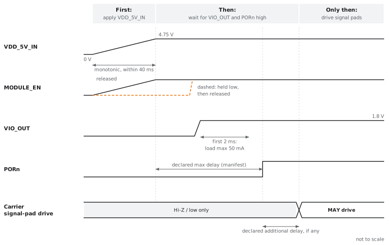
(informative): Power-up order (§6.2.1), not to scale. The carrier drives the signal pads only after VIO_OUT and PORn are high and any declared additional delay has passed.
6.2.2 Power-down
- First, the carrier SHOULD request a graceful shut-down by the means the SoM manifest declares (application link, a GPIO, or
MODULE_STBY) and give the SoM time to finish writes to non-volatile memory. - Next, when
PORnfalls, the carrier SHALL set every output that drives a SoM signal pad to high impedance or low within 1 ms (E1M-AEN only). - Then, if the SoM has not powered off by itself, the carrier forces power-off with
MODULE_ENlow (§6.3.1). - Last, the carrier removes
VDD_5V_IN. It SHOULD wait untilVIO_OUTis low before it removesVDD_5V_IN.
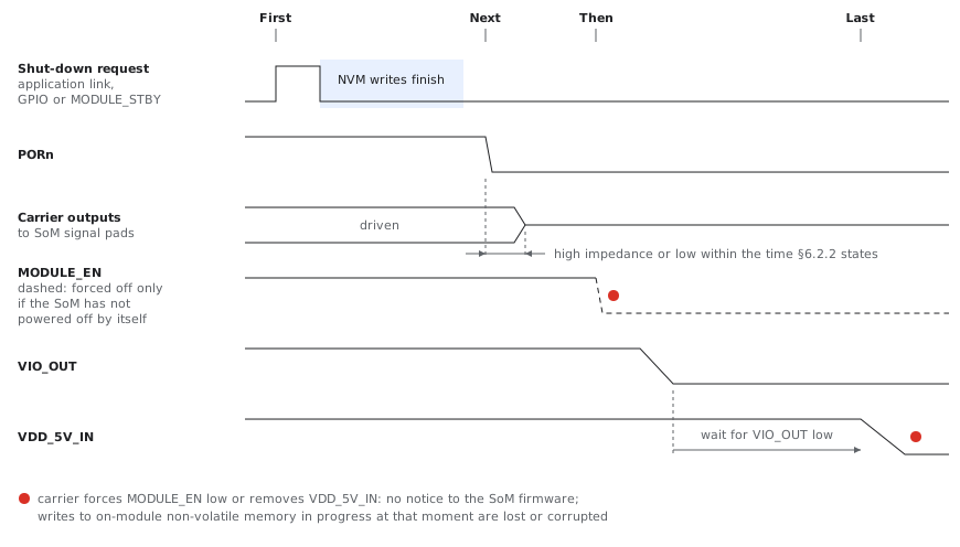
(informative): Power-down order (§6.2.2), not to scale. The red marks are the paths that give the SoM firmware no notice.
Pulling MODULE_EN low, pulling PORn low and removing VDD_5V_IN give the SoM firmware no notice. Writes to on-module non-volatile memory that are in progress at that moment are lost or corrupted.
6.2.3 Back-powering and I/O gating
- No drive into an unpowered SoM. While
VIO_OUTis low, the carrier SHALL NOT drive anyVIO_OUT-domain signal pad (§6.7.1) high and SHALL NOT source current into it, whether from a push-pull output, a pull-up resistor, a debug probe, a USB-to-UART bridge or any other carrier circuit. Pull-down resistors, and open-drain outputs that only pull low, are permitted at any time. - Exceptions. Clause 1 does not apply to
MODULE_EN(5 V tolerant, §6.3.1), toIO25when the SoM uses it asRTC_WAKE_N(open-drain, 5 V tolerant, §8.2), or to pads in a domain other thanVIO_OUT; those pads follow the rule in §6.7.1. Clause 4 does not apply toRTC_WAKE_Neither: its pull-up goes to an always-on rail. - Gate. The carrier SHALL use
VIO_OUThigh together withPORnhigh as the condition for drivingVIO_OUT-domain signal pads (§6.2.1 and §6.2.2). - Pull-up rail. Every carrier pull-up on a
VIO_OUT-domain pad SHALL go toVIO_OUTor to a carrier rail switched byVIO_OUT(§6.1.2 clause 3), never to an always-on rail. - Level. The carrier SHALL keep every
VIO_OUT-domain pad between −0.3 V and 1.98 V (absolute maximum of the 1.8 V pads of both E1M-AEN and E1M-X V2N / V2N-M1). - Debug probes. A debug probe or console adapter on the SoM's debug pads (§7.3.10, §7.3.13) SHALL use
VIO_OUTas its target reference, SHALL have its target-power output disabled, and SHALL keep its outputs high-impedance whileVIO_OUTis low. - Switched pad groups. Where a SoM supplies a group of its
VIO_OUT-domain pads from an internal rail that can be off whileVIO_OUTis high (for example the pads of an on-module radio), it SHALL list those pads in its manifest, and the carrier SHALL apply clause 1 to them while that rail is off.
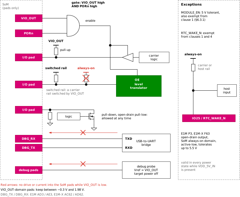
(informative): Carrier I/O gating and back-powering. Carrier drivers into VIO_OUT-domain pads are enabled by VIO_OUT high together with PORn high (clause 3); pull-ups go to VIO_OUT or a rail switched by it (clause 4); MODULE_EN and IO25 / RTC_WAKE_N are the exceptions of clause 2.
6.3 Reset and module enable
| Pad | Direction | Polarity | Description |
|---|---|---|---|
MODULE_EN | input | active-high (default high via SoM-internal pull-up) | Drive low to switch the SoM off and hold it off; release to switch it on. 5 V tolerant. Open-drain drive. Carrier MAY leave floating if not used. Drive rules: §6.3.1. |
MODULE_STBY | input | active-low (default high via SoM-internal pull-up) | Module standby (low-power) request. The protocol (level or pulse) is declared in the per-SoM manifest. Not 5 V tolerant on every SoM. Open-drain drive. Carrier MAY leave floating if not used. Drive rules: §6.3.1. |
PORn | input, open-drain, wired-AND | active-low (default high via SoM-internal pull-up to 1.8 V) | Power-on reset. Drive low to reset the SoM. A SoM MAY also hold it low itself while its rails are not valid. Carrier MAY leave floating if not used. Drive rules: §6.3.1. |
A SoM SHALL power up and boot when VDD_5V_IN is applied with MODULE_EN, MODULE_STBY and PORn all left unconnected. None of these pads needs a carrier pull-up.
6.3.1 Control-pad drive rules
- MODULE_EN. A SoM SHALL tolerate any voltage from −0.3 V to 5.5 V on
MODULE_ENand MAY pull it up internally to a rail as high asVDD_5V_IN. The carrier SHALL pullMODULE_ENlow only with an open-drain or open-collector output, a switch or a push-button toGND; push-pull drive is permitted only towards SoMs whose manifest allows it. The carrier SHALL NOT fit a pull-up onMODULE_ENto a rail that can be off whileVDD_5V_INis present, and SHALL NOT connectMODULE_ENdirectly to a GPIO of a host that can be unpowered while the SoM must stay on (the unpowered host clamps the line low); such a host SHALL driveMODULE_ENthrough a buffer, for example an N-MOSFET toGND. Every carrier part onMODULE_EN(buffer transistor, ESD diode, read-back input) SHALL be rated for 5.5 V. With the carrier driver released, the total carrier leakage onMODULE_ENSHALL NOT exceed 0.1 µA (E1M-AEN only; its internal pull-up is about 1 MΩ).MODULE_ENlow is a hard power cut and SHOULD NOT be used as the normal power-off path (§6.2.2). - MODULE_STBY. The carrier SHALL pull
MODULE_STBYlow only with an open-drain output, a switch or a push-button toGND, and SHALL NOT fit a pull-up on it to any rail other thanVIO_OUT. With the carrier driver released, the total carrier leakage onMODULE_STBYSHALL NOT exceed 0.1 µA (E1M-AEN only). A SoM SHALL declare in its manifest the standby protocol (level or pulse) and the minimum low and high times. - PORn. The carrier SHALL pull
PORnlow only with an open-drain output, a switch or a push-button toGND, SHALL NOT drive it high, and SHALL NOT fit a pull-up on it. The carrier SHALL holdPORnlow for at least the minimum the SoM declares, and for at least 2 ms when it targets any SoM (E1M-AEN only; E1M-X V2N / V2N-M1: TBD). The carrier SHALL NOT add more than 1 nF onPORn(E1M-AEN only). A carrier input that readsPORnSHALL be high-impedance while its own supply is off. - JTAG_nRST. The carrier SHALL pull
JTAG_nRSTlow only with an open-drain output and SHALL NOT fit a pull-up on it to any rail other thanVIO_OUT.
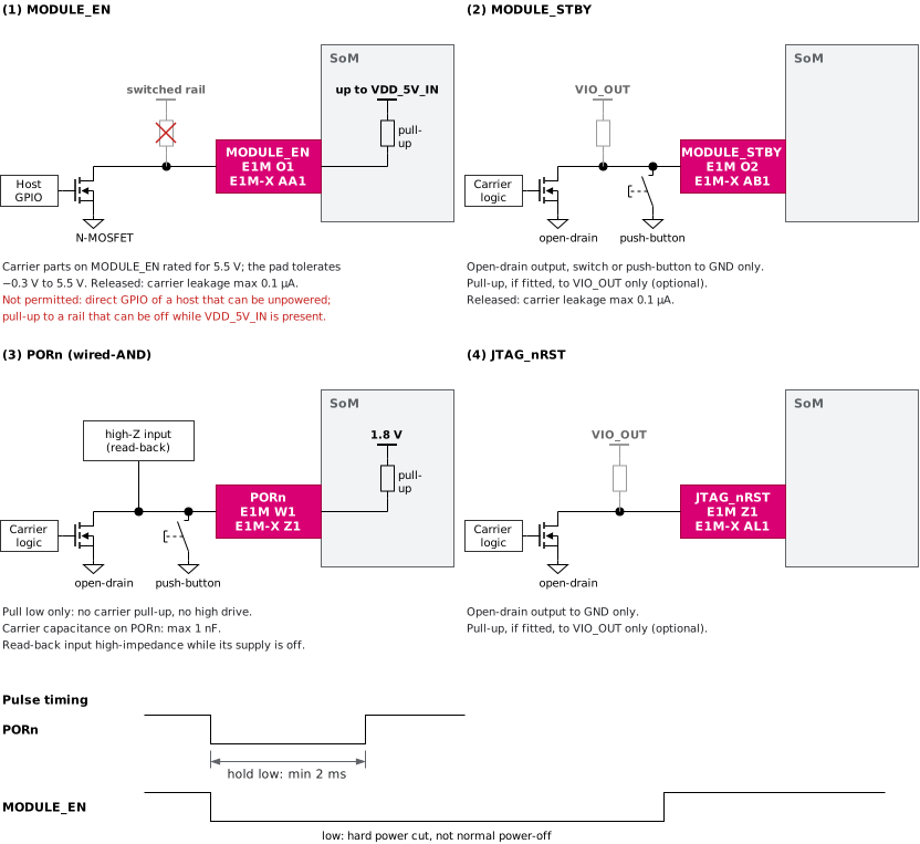
(informative): Carrier drive circuits for the control pads (§6.3.1) and the PORn and MODULE_EN low pulses.
6.4 Boot configuration
E1M and E1M-X define a four-pin boot strap on BOOT0, BOOT1, BOOT2, and BOOT3.
- Pads. A conformant SoM SHALL expose
BOOT0–BOOT3on its footprint at the pad locations of §7.3.1 and SHALL NOT assign any other function to those pads. - Interpretation. The interpretation of the strap is silicon-specific and SHALL be declared in the per-SoM manifest.
- Ignored strap. A SoM whose boot does not depend on the strap MAY ignore
BOOT0–BOOT3(for example, leave the pads unconnected on the module). Such a SoM SHALL declare in its manifest that it ignores the strap, and SHALL tolerate any carrier strap circuit that meets clause 4. - Carrier. A carrier board MAY fit a strap circuit on
BOOT0–BOOT3whatever SoM it targets. Its pull-ups SHALL go toVIO_OUTor to a carrier rail switched byVIO_OUT(§6.2.3). On a SoM that declares the strap ignored, the circuit has no effect, so a carrier that hosts several SoMs keeps the same strap circuit for all of them.
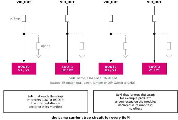
(informative): Carrier strap circuit on BOOT0–BOOT3 (§6.4). The same circuit serves a SoM that reads the strap and a SoM that ignores it.
BOOT0–BOOT3 unconnected on the module, boots from on-chip MRAM and declares the strap ignored (Annex A.1); it is conformant to this clause.
The reference mapping below applies to the rev 1.0 reference SoMs based on Renesas RZ/V2N (informative).
| BOOT1 | BOOT0 | Boot mode | Device | CA55 boot | CM33 boot |
|---|---|---|---|---|---|
| 0 | 0 | Mode 0 | eSD (3.3 V) | Supported | Not supported |
| 0 | 1 | Mode 1 | eMMC (1.8 V I/O) | Supported | Not supported |
| 1 | 0 | Mode 2 | QSPI NOR (1.8 V I/O) | Supported | Supported |
| 1 | 1 | Mode 3 | SCIF download | Supported | Supported |
BOOT2 is fixed at 1 on the rev 1.0 reference SoMs; carrier boards SHALL drive it according to the SoM manifest's declared default or leave it as the SoM's internal pull defines. BOOT3 selects the boot CPU on the reference SoMs (high → CA55, low → CM33).
6.5 Mandatory on-module components
The E1M pinout is designed around a SoM that integrates the following functions on the module itself, so that carrier-board designers do not have to repeat them:
| Component | Requirement |
|---|---|
| Ethernet PHY(s) | A conformant SoM SHALL include at least one on-module Ethernet PHY connected to the SoC's MAC and exposed on the carrier board via the PHY-side (pre-magnetics) differential MDI pads (ETH0_* minimum). SoMs whose SoC supports two MACs SHALL populate a second on-module PHY and expose ETH1_*. The SoM SHALL declare in its manifest the highest link rate of each port (§7.3.6). |
| Wi-Fi + Bluetooth combo | A conformant SoM SHALL include an on-module Wi-Fi 6 (IEEE 802.11ax) and Bluetooth 5.4 combo radio. 2.4 GHz operation is REQUIRED. 5 GHz operation and 6 GHz operation are each OPTIONAL; the SoM SHALL declare in its manifest the Wi-Fi bands it supports. |
| Antenna outputs | The SoM SHALL drive ANT_2.4GHz (§7.3.2). It SHALL drive ANT_5GHz and ANT_6GHz only for a band it supports and uses on that pad. A SoM that does not use ANT_5GHz or ANT_6GHz SHALL leave that pad no-connect on the module and SHALL declare it in its manifest. Informative: E1M-AEN (2.4 GHz only) drives ANT_2.4GHZ and leaves ANT_5GHZ and ANT_6GHZ no-connect; it is conformant. |
| CAN transceiver(s) | If the SoM exposes the CAN pads of a CAN group (§7.3.14), it SHALL implement that group in one of two options and SHALL declare the option for each group in its manifest. Bus-level CAN (the default): the SoM includes an on-module CAN transceiver, and the pads carry the bus side (CANxH, CANxL), suitable for direct connection to a terminator and a CAN connector. Logic-level CAN (declared option): the SoM has no on-module transceiver for that group, the pads carry the controller side (CANx_TX, CANx_RX) in the VIO_OUT (1.8 V) domain, and the carrier provides the transceiver (§7.3.14). |
Carrier-board designers SHALL NOT add an external Ethernet PHY, Wi-Fi/BLE module, or CAN transceiver between the carrier and any of these signal classes; the carrier provides only the magnetics + RJ-45 (for Ethernet), antenna routing or external antenna connector (for Wi-Fi / BLE), and bus termination + connector (for CAN). The one exception is a CAN group that the SoM declares as logic-level CAN: for that group the carrier SHALL provide the transceiver (§7.3.14).
This is a family-wide invariant: it applies to every conformant E1M and E1M-X SoM regardless of which SoC silicon the SoM uses.
6.6 Electrical characteristics
The values below are fixed by this revision; each row points to the clause that makes it normative.
| Parameter | Value | Clause |
|---|---|---|
VDD_5V_IN operating window at the pads | 4.75–5.25 V | §6.1.1 (1), (9) |
VDD_5V_IN absolute maximum (carrier limit; SoM withstand) | 5.5 V | §6.1.1 (2), (9) |
VDD_5V_IN ramp, 0 V to 4.75 V | monotonic, ≤ 40 ms (E1M-AEN only) | §6.1.1 (3), (9) |
VIO_OUT level | 1.8 V nominal, ±5 % (tolerance: E1M-X V2N / V2N-M1 only) | §6.1.2 (1) |
VIO_OUT carrier load, any SoM | ≤ 100 mA; ≤ 50 mA in the first 2 ms; ≤ 2.5 µF (E1M-AEN only) | §6.1.2 (4) |
VIO_OUT-domain signal pads | −0.3 V to 1.98 V | §6.2.3 (5) |
Carrier outputs Hi-Z or low after PORn falls | ≤ 1 ms (E1M-AEN only) | §6.2.2 (2) |
MODULE_EN voltage range the SoM tolerates | −0.3 V to 5.5 V | §6.3.1 (1) |
MODULE_EN, MODULE_STBY released carrier leakage | ≤ 0.1 µA (E1M-AEN only) | §6.3.1 (1), (2) |
PORn carrier low pulse, any SoM | ≥ 2 ms (E1M-AEN only) | §6.3.1 (3) |
PORn carrier capacitance | ≤ 1 nF (E1M-AEN only) | §6.3.1 (3) |
The four tables below collect, by signal class, the absolute maximum ratings, recommended operating conditions, DC characteristics and AC characteristics. They are informative: they restate values that §6.1–§6.7, §8.2 and Annex A already state, with the same provenance marks, and add no requirement. Where a table and a clause differ, the clause governs. A row that reads "per SoM datasheet" has no value in this revision; the SoM datasheet and manifest give it.
| Signal class | Parameter | Value | Clause / provenance |
|---|---|---|---|
| Supply input | VDD_5V_IN voltage at the pads | ≤ 5.5 V, including transients | §6.1.1 (2), (9) |
| Control | MODULE_EN voltage | −0.3 V to 5.5 V | §6.3.1 (1) |
| Control | IO25 used as RTC_WAKE_N, voltage | ≤ 5.5 V (5 V tolerant); minimum per SoM datasheet | §8.2 |
VIO_OUT-domain signal pads | Voltage at any VIO_OUT-domain pad (§6.7.1) | −0.3 V to 1.98 V | §6.2.3 (5) |
| SD card pads | SD_CLK, SD_CMD, SD_D0–SD_D3 voltage | per SoM datasheet | §6.7.1 |
| High-speed and RF pads | USB, MIPI CSI / DSI, PCIe, Ethernet MDI, ANT_* | per SoM datasheet | §6.7.1 |
| Module | Storage temperature, ESD rating | per SoM datasheet | — |
| Signal class | Parameter | Value | Clause / provenance |
|---|---|---|---|
| Supply input | VDD_5V_IN voltage at the pads | 4.75–5.25 V (5 V nominal) | §6.1.1 (1), (9) |
| Supply input | VDD_5V_IN peak input current | as the SoM declares; 834 mA (E1M-AEN801, calculated) | §6.1.1 (5), (9); value (informative: E1M-AEN, DS-AEN-001) |
| Supply input | Carrier bulk capacitance at VDD_5V_IN | as the SoM declares; ≥ 50 µF effective per A of total VDD_5V_IN load | §6.1.1 (7); value (informative: E1M-AEN, DS-AEN-001) |
| Supply output | VIO_OUT total carrier load current | ≤ 100 mA | §6.1.2 (4) (E1M-AEN only) |
| Supply output | VIO_OUT carrier load current, first 2 ms after VIO_OUT rises | ≤ 50 mA | §6.1.2 (4) (E1M-AEN only) |
| Supply output | VIO_OUT total external capacitance | ≤ 2.5 µF | §6.1.2 (4) (E1M-AEN only) |
| Control | MODULE_EN, MODULE_STBY carrier leakage, driver released | ≤ 0.1 µA | §6.3.1 (1), (2) (E1M-AEN only) |
| Control | PORn carrier capacitance | ≤ 1 nF | §6.3.1 (3) (E1M-AEN only) |
VIO_OUT-domain signal pads | Signal level | VIO_OUT (1.8 V nominal); input thresholds per SoM datasheet | §6.1.2 (1), §6.7.1 |
| SD card pads | Signal level | SD_VDD_OUT / SD_VDD levels, only while that rail is on | §6.7.1 |
| Module | Ambient operating temperature | −40 to +75 °C (E1M-AEN); −40 to +85 °C (E1M-X V2N / V2N-M1) | (informative: Annex A.1, A.2, A.3) |
| Signal class | Parameter | Value | Clause / provenance |
|---|---|---|---|
| Supply input | On-module input capacitance at VDD_5V_IN | about 50 µF | §6.1.1 (9); value (informative: E1M-AEN, DS-AEN-001) |
| Supply output | VIO_OUT output voltage | 1.8 V nominal, ±5 % | §6.1.2 (1); tolerance (E1M-X V2N / V2N-M1 only; E1M-AEN TBD) |
| Supply output | SD_VDD_OUT / SD_VDD output voltage | 3.4 V (E1M-AEN, hw_rev R3); 1.8 V / 3.3 V, switched automatically (E1M-X V2N / V2N-M1) | §6.7.1 (informative) |
| Supply output | BL_LED_A voltage | up to 36 V (KTD2801 over-voltage limit) | §6.7.1; value (informative: E1M-AEN, DS-AEN-001) |
| Control | MODULE_EN SoM-internal pull-up | to a rail up to VDD_5V_IN; about 1 MΩ | §6.3, §6.3.1 (1); value (E1M-AEN only) |
| Control | MODULE_STBY SoM-internal pull-up | present; value per SoM datasheet | §6.3 |
| Control | PORn SoM-internal pull-up | to 1.8 V; value per SoM datasheet | §6.3 |
| Control | IO25 used as RTC_WAKE_N output | open-drain, active-low; output low level per SoM datasheet | §8.2 |
VIO_OUT-domain signal pads | VIL, VIH, VOL, VOH, drive strength, leakage | per SoM datasheet | — |
| Signal class | Parameter | Value | Clause / provenance |
|---|---|---|---|
| Supply input | VDD_5V_IN rise, 0 V to 4.75 V | monotonic, ≤ 40 ms | §6.1.1 (3), (9) (E1M-AEN only) |
| Control | VDD_5V_IN at 4.75 V, or MODULE_EN release, to PORn high | maximum as the SoM declares; 206 ms typical, 290 ms maximum (E1M-AEN) | §6.2.1; value (informative: E1M-AEN, DS-AEN-001) |
| Control | PORn carrier low pulse, any SoM | ≥ 2 ms | §6.3.1 (3) (E1M-AEN only) |
| Control | MODULE_STBY minimum low and high times | as the SoM declares; value per SoM datasheet | §6.3.1 (2) |
VIO_OUT-domain signal pads | PORn falling to carrier outputs high-impedance or low | ≤ 1 ms | §6.2.2 (2) (E1M-AEN only) |
VIO_OUT-domain signal pads | Interface timing (I2C, SPI, UART, I2S, SDIO and others) | per SoM datasheet | — |
6.7 Pad voltage domains and safe default fits
6.7.1 Pad voltage domains
Unless listed below, every signal pad of a conformant SoM is in the VIO_OUT (1.8 V) domain, and §6.2.3 applies to it. The pads below are in another domain. The carrier SHALL NOT clamp them to VIO_OUT, pull them up to VIO_OUT or level-translate them as 1.8 V signals, and SHALL apply the rule given for each.
VIO_OUT domain| Pads | Domain | Carrier rule |
|---|---|---|
MODULE_EN | up to 5.5 V | §6.3.1 (1). |
VDD_5V_IN / VDD | 5 V input | §6.1.1. |
VIO_OUT, SD_VDD_OUT / SD_VDD, +V_CAM0–+V_CAM3 | SoM supply outputs | The carrier SHALL NOT drive, back-feed or connect another supply to them. Informative: on E1M-AEN, SD_VDD was a carrier input on hw_rev R2 and is a 3.4 V SoM output from hw_rev R3. |
SD_CLK, SD_CMD, SD_D0–SD_D3 | SD_VDD_OUT / SD_VDD | The carrier SHALL drive or pull them up only to SD_VDD_OUT / SD_VDD levels and only while that rail is on. Informative: E1M-AEN 3.4 V through an on-module translator; E1M-X V2N / V2N-M1 1.8 V / 3.3 V, switched automatically. |
BL_LED_A, BL_LED_K | backlight LED string | The carrier SHALL connect only an LED string (anode on BL_LED_A) and its feedback network; it SHALL NOT connect a logic input or another supply. Informative: E1M-AEN BL_LED_A reaches up to 36 V (KTD2801 over-voltage limit). |
ETH0_*, ETH1_* MDI pairs | PHY MDI | §7.3.6. |
ANT_* | RF | §7.3.2. |
USB* data, USB*_VBUS, USB_CC1, USB_CC2 | USB | Per the USB specifications. |
CSI*, DSI*, PCIE* | high-speed differential | Per the MIPI and PCIe specifications. |
CANxH/CANx_TX, CANxL/CANx_RX | bus level, or VIO_OUT domain, per the declared CAN option | §6.7.2 and §7.3.14. |
+S_CAP | RTC backup store | As declared in the per-SoM manifest. |
A SoM SHALL declare in its manifest any other pad that is not in the VIO_OUT domain, with its domain.
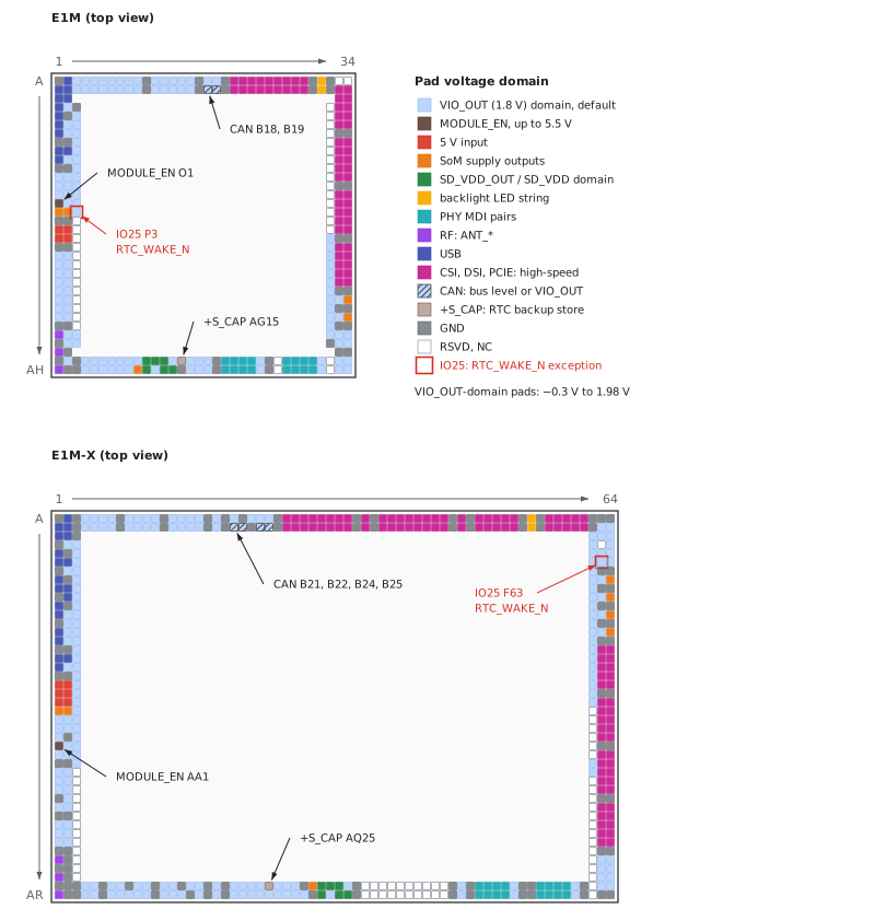
(informative): Pad voltage domains on the E1M and E1M-X pad maps, generated from pinout/v1.json and pinout/x-v1.json (top view). Pads not listed in the table above are in the VIO_OUT domain.
6.7.2 Safe default fits for dual-meaning pads
The CAN pads (§7.3.14) carry either bus-level signals or 1.8 V logic signals, depending on the CAN option the SoM declares. A carrier that supports both options on one PCB uses assembly options (BOM variants, 0 Ω links or not-fitted parts).
- Safe default. For every group of dual-meaning pads, the carrier's default assembly (the fit used when no SoM set is declared) SHALL be the fit that cannot damage any conformant SoM.
- CAN default. For the CAN pads, the default assembly SHALL be the carrier-transceiver path: the carrier transceiver connected to the CAN pads, and the bypass path that connects the CAN pads straight to the bus connector, termination or bus-side protection not fitted (DNP). Bus voltages on logic-level CAN pads destroy the SoC: on the E1M-AEN standard build these are 1.8 V SoC pads with an absolute maximum of −0.3 V to 1.98 V.
- Bypass fit. The carrier MAY fit the bypass path, with the carrier transceiver out of circuit, only in a build variant that declares (§9.2) a SoM set in which every SoM declares bus-level CAN for the CAN groups concerned. With a bus-level SoM on the default assembly, CAN does not work until the bypass variant is fitted.
- Mutual exclusion. The carrier-transceiver path and the bypass path of the same CAN group SHALL NOT both be fitted.
- Declaration. Every carrier build variant SHALL declare which fit it uses for each dual-meaning pad group and which SoMs it supports.
7 Pinout
7.1 Pin numbering convention
Pads on each form factor SHALL be identified using a BGA-style coordinate of the form <row-letter(s)><column-number>, in the top view (component side up):
A1is the corner pad at row A, column 1, of the form factor's coordinate space: the top-left corner pad, next to the pin-1 fiducial.- Row letters increase from the top edge as
A, B, …, Z, AA, AB, …, AHfor E1M andA, B, …, Z, AA, AB, …, ARfor E1M-X.B1is directly belowA1. - Column numbers increase from the left edge,
1–34for E1M and1–64for E1M-X.A2is directly right ofA1. - The E1M-X outline is therefore 65 mm across (columns
1–64) and 45 mm down (rowsA–AR). - The pad band is two pads deep along the top and bottom edges (rows
A,BandAG,AHon E1M;A,BandAQ,ARon E1M-X) and three pads deep along the left and right edges (columns1–3and32–34on E1M;1–3and62–64on E1M-X).
Each form factor uses its own coordinate space; the same physical pad position has different coordinates on E1M and E1M-X. The form-factor identifier E1M or E1M-X distinguishes the two.
The pad maps follow the same frame: top view, letters on the rows (top to bottom), numbers on the columns (left to right); every pad is drawn at the crossing of its row and its column. Both maps are split into quarters, the E1M map in Figure 20, Figure 21, Figure 22 and Figure 23, the E1M-X map in Figure 24, Figure 25, Figure 26 and Figure 27. The four quarters of a map print at the same scale, and the split keeps every pad name legible.
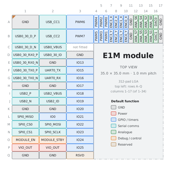
E1M pad map (top view), top left: rows A–Q, columns 1–17
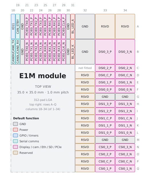
E1M pad map (top view), top right: rows A–Q, columns 18–34
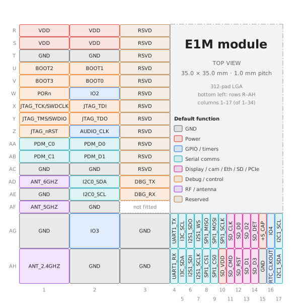
E1M pad map (top view), bottom left: rows R–AH, columns 1–17
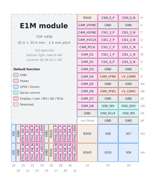
E1M pad map (top view), bottom right: rows R–AH, columns 18–34
pinout/v1.json). Rows A–AH (34 letters, top to bottom) × columns 1–34 (left to right); A1 top left, A2 right of A1, B1 below A1. The bands of rows A, B and AG, AH are two pads deep; the side bands of columns 1–3 and 32–34 are three pads deep; pads C3, AF3, C32 and AF32 are not fitted. Pad cells are coloured by the pad's default function. Centre is reserved for top-side components per §5.3.
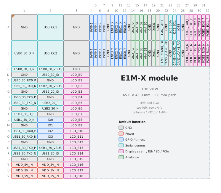
E1M-X pad map (top view), top left: rows A–V, columns 1–32
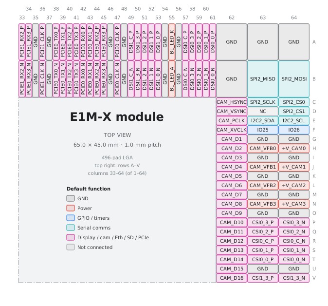
E1M-X pad map (top view), top right: rows A–V, columns 33–64
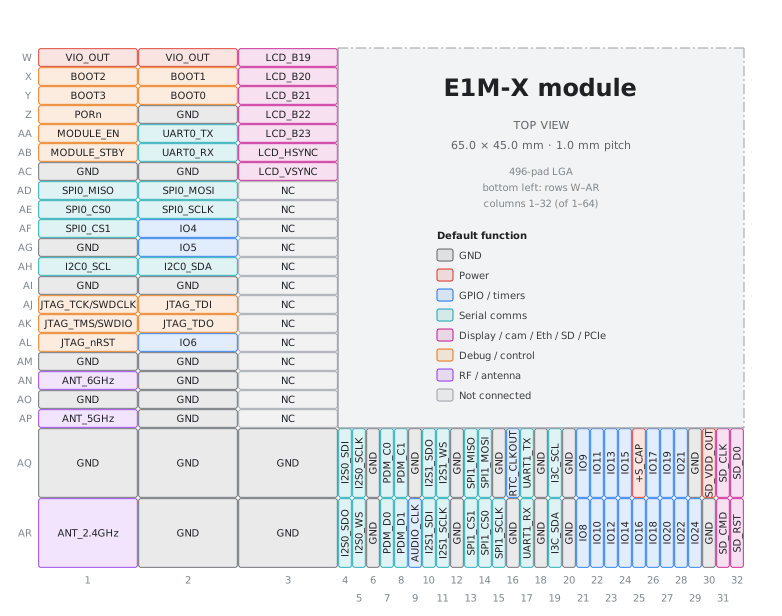
E1M-X pad map (top view), bottom left: rows W–AR, columns 1–32
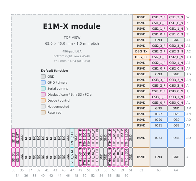
E1M-X pad map (top view), bottom right: rows W–AR, columns 33–64
pinout/x-v1.json). Rows A–AR (44 letters, top to bottom, along the 45 mm side) × columns 1–64 (left to right, along the 65 mm side); A1 top left, A2 right of A1, B1 below A1. The pad band is two pads deep along the long edges (rows A, B, AQ, AR) and three pads deep along the short edges (columns 1–3 and 62–64). Pad cells are coloured by the pad's default function.
7.2 Interface count overview
The following table summarises the count of each peripheral interface exposed by this standard on each form factor.
| Feature | E1M | E1M-X |
|---|---|---|
| Ethernet port (MDI, up to 1000BASE-T) | 2 | 2 |
| USB 2.0 | 1 | 1 |
| USB 3.x | 1 | 2 |
| UART | 2 | 2 |
| Debug UART (console) | 1 | 1 |
| SPI | 2 | 3 |
| I2C | 2 | 4 |
| I3C | 1 | 1 |
| I2S | 2 | 2 |
| SDIO / SD card (4-bit) | 1 | 1 |
| CAN-BUS | 1 | 2 |
| JTAG / SWD | 1 | 1 |
| GPIO (default-function) | 23 | 34 |
| PDM microphone | 2 | 2 |
| Audio master clock | 1 | 1 |
| RTC clock output | 1 | 1 |
| Boot-strap pins | 4 | 4 |
| Analogue input (ADC) | 8 | 8 |
| Analogue output (DAC) | 2 | 2 |
| Quadrature encoder | 4 | 4 |
| PWM | 8 | 8 |
| MIPI CSI-2 4-lane | 2 | 4 |
| MIPI DSI 4-lane | 2 | 2 |
| Parallel camera (8 / 16-bit) | 1 (8 bit) | 1 (16 bit) |
| Parallel LCD (24-bit RGB) | — | 1 |
| PCIe 4-lane | 1 | 2 |
| Reserved (RSVD) | 34 | 20 |
| Not connected (NC) | 0 | 34 |
The "GPIO (default-function)" row counts only pads whose default signal is GPIO. Per §8.2, every digital pad (USB, MIPI, ADC, etc.) MAY also be repurposed as GPIO on a conformant SoM; those repurposings are not counted here. The "Ethernet port" row counts MDI pad groups; each group has the four pairs that 1000BASE-T needs, and the link rate a SoM supports is declared in its manifest (§7.3.6). The debug UART is not counted in the "UART" row.
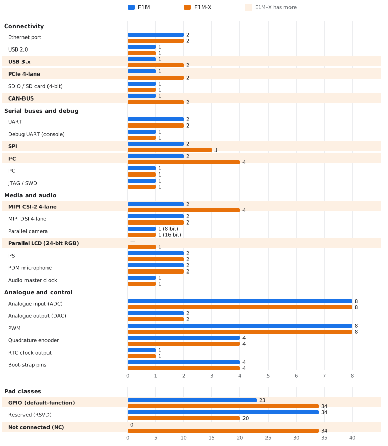
(informative): Interface counts per form factor, from the table above. Shaded rows: E1M-X has more instances, or is the only form factor with the interface. GPIO, RSVD and NC pads are drawn on their own scale.
7.3 Pad assignments
Each subsection below is normative for the pad-to-signal mapping listed. Pad coordinates are given for both form factors; an empty column ("E1M only" or "E1M-X only") means the pad does not exist on the other form factor. The pin name in the third column is the silkscreen on the SoM and matches the silkscreen field of the corresponding JSON pad. Where the silkscreen text differs between the two form factors (because of historical naming choices in the Altium project), both names are shown. Slash-combo names (JTAG_TCK/SWDCLK, CAN0H/CAN0_TX) carry two equally-conformant primary functions; see §8.3.
7.3.1 Power & control
| E1M-X coord(s) | E1M coord(s) | Pin name |
|---|---|---|
| AQ25 | AG15 | +S_CAP |
| H64 | Z34 | +V_CAM0 |
| J64 | AB34 | +V_CAM1 |
| L64 | (E1M-X only) | +V_CAM2 |
| N64 | (E1M-X only) | +V_CAM3 |
| AR9 | Z2 | AUDIO_CLK |
| B55 | A31 | BL_LED_A |
| A55 | B31 | BL_LED_K |
| Y2 | V2 | BOOT0 |
| X2 | U2 | BOOT1 |
| X1 | U1 | BOOT2 |
| Y1 | V1 | BOOT3 |
| H63 | Z33 | CAM_VFB0 |
| J63 | AB33 | CAM_VFB1 |
| L63 | (E1M-X only) | CAM_VFB2 |
| N63 | (E1M-X only) | CAM_VFB3 |
105 pads (see pinout/x-v1.json) | 49 pads (see pinout/v1.json) | GND |
| AA1 | O1 | MODULE_EN |
| AB1 | O2 | MODULE_STBY |
| Z1 | W1 | PORn |
| AQ16 | AH16 | RTC_CLKOUT |
| T1, T2, U1, U2, V1, V2 | R1, R2, S1, S2 | VDD_5V_IN (E1M-X) / VDD (E1M) |
| W1, W2 | P1, P2 | VIO_OUT |
The complete GND pad list is enumerated in pinout/v1.json (E1M) and pinout/x-v1.json (E1M-X). Carrier boards SHALL connect every GND pad of the SoM to a low-impedance ground plane.
7.3.2 Antenna
Antenna outputs are driven by the SoM's on-module Wi-Fi 6 + BLE 5.4 combo radio (mandatory per §6.5). A conformant SoM SHALL populate ANT_2.4GHz. ANT_5GHz and ANT_6GHz are OPTIONAL: a SoM populates each only for a band it supports, and a SoM that does not use one of them leaves it no-connect and declares it in its manifest (§6.5). Pads not driven by the on-module radio SHALL be left as no-connect by the carrier board; a carrier that hosts more than one SoM implements this per build variant, for example with a not-fitted link at the pad. Where used, the carrier-board trace SHALL be 50 Ω characteristic impedance.
| E1M-X coord(s) | E1M coord(s) | Pin name |
|---|---|---|
| AR1 | AH1 | ANT_2.4GHz (E1M-X) / ANT_2.4GHZ (E1M) |
| AP1 | AF1 | ANT_5GHz (E1M-X) / ANT_5GHZ (E1M) |
| AN1 | AD1 | ANT_6GHz (E1M-X) / ANT_6GHZ (E1M) |
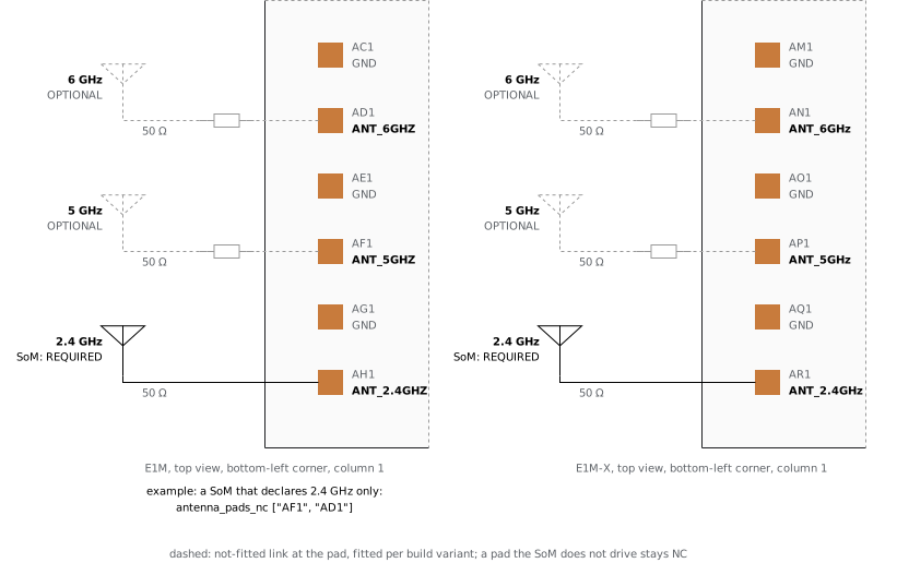
(informative): Antenna pads (§7.3.2) and carrier routing at the bottom-left corner of each form factor, top view: the pads are in column 1, rows AC–AH (E1M) and AM–AR (E1M-X), next to the left edge.
7.3.3 Reserved (RSVD)
Reserved pads are reserved for manufacturing or future expansion. Carrier boards SHALL leave them unconnected: no trace, test point, pull resistor, load or jumper. An RSVD pad can carry a live on-module net used in production, and connecting it can damage the SoM. Informative: on E1M-AEN, W3 is an on-module 1.8 V rail and U3 / V3 are a 3.3 V programming port.
| E1M-X coord(s) | E1M coord(s) | Pin name |
|---|---|---|
| W62, X62, Y62, Z62, AA62, AB62, AE62, AF62, AG62, AH62, AI62, AJ62, AK62, AL62, AM62, AN62, AO62, AP62, AQ62, AR62 | A33, A34, D32, E32, F32, G32, H32, I32, J32, K32, L32, M32, N32, O32, P32, Q3, Q32, R3, R32, S3, T3, U3, V3, W3, X3, Y3, Z3, AA3, AB3, AC3, AG26, AG32, AH26, AH32 | RSVD |
7.3.4 Not connected (NC)
NC pads have no internal connection. Carrier boards MAY route through them or leave them unconnected. This permission applies only to pads whose default function in this specification is NC. A pad that one SoM does not route (listed in its manifest not_routed, or described as "NC" in a SoM datasheet) keeps its standard function on other SoMs; a carrier that targets the standard generically SHALL NOT route unrelated nets through such a pad.
| E1M-X coord(s) | E1M coord(s) | Pin name |
|---|---|---|
| D63, AD3, AE3, AF3, AG3, AH3, AI3, AJ3, AK3, AL3, AM3, AN3, AO3, AP3, AQ36– AQ45, AR36– AR45 | (none) | NC |
7.3.5 USB
E1M provides one USB 2.0 and one USB 3.x interface. E1M-X provides one USB 2.0 and two USB 3.x interfaces.
| E1M-X coord(s) | E1M coord(s) | Pin name |
|---|---|---|
| C1 | C1 | USB0_30_D_N |
| B1 | B1 | USB0_30_D_P |
| D2 | D2 | USB0_30_ID |
| F1 | E1 | USB0_30_RX0_N |
| E1 | D1 | USB0_30_RX0_P |
| I1 | G1 | USB0_30_TX0_N |
| H1 | F1 | USB0_30_TX0_P |
| C2 | C2 | USB0_30_VBUS (E1M-X) / USB0_VBUS (E1M) |
| L1 | (E1M-X only) | USB1_30_D_N |
| K1 | (E1M-X only) | USB1_30_D_P |
| R2 | (E1M-X only) | USB1_30_ID |
| O1 | (E1M-X only) | USB1_30_RX0_N |
| N1 | (E1M-X only) | USB1_30_RX0_P |
| R1 | (E1M-X only) | USB1_30_TX0_N |
| Q1 | (E1M-X only) | USB1_30_TX0_P |
| Q2 | (E1M-X only) | USB1_30_VBUS |
| J2 | J1 | USB2_20_N (E1M-X) / USB2_N (E1M) |
| I2 | I1 | USB2_20_P (E1M-X) / USB2_P (E1M) |
| G2 | J2 | USB2_20_ID (E1M-X) / USB2_ID (E1M) |
| F2 | I2 | USB2_20_VBUS (E1M-X) / USB2_VBUS (E1M) |
| A2 | A2 | USB_CC1 |
| B2 | B2 | USB_CC2 |
7.3.6 Ethernet
E1M and E1M-X each integrate on-module Ethernet PHY(s) (mandatory per §6.5) connected to the SoC MAC(s) via SoM-internal RGMII / RMII; the differential MDI pads exposed to the carrier board are post-PHY and pre-magnetics. Carrier boards SHALL provide a magnetic transformer (or transformer-integrated RJ-45 connector) for each port they use and SHALL NOT add an external PHY.
- Routing. The carrier SHALL route each MDI pair as a 100 Ω differential pair.
- ESD. The carrier SHALL provide ESD protection on the MDI lines of every port it brings to a connector (a low-capacitance ESD array between the magnetics and the connector, with a common-mode choke where needed). A SoM MAY also include MDI ESD protection and SHALL declare in its manifest whether it does. Informative: the E1M-AEN PHY (TI DP83825) integrates ±5 kV IEC 61000-4-2 ESD on its MDI pins; the E1M-X V2N / V2N-M1 MDI lines have no on-module EMI/ESD protection.
- Link rate. Each
ETHxgroup has the four MDI pairs (DA–DD) that 1000BASE-T needs. A SoM SHALL declare the highest link rate of each port in its manifest. A SoM whose port supports only 100BASE-TX uses theDAandDBpairs and MAY leaveDCandDDunconnected. A carrier that hosts any SoM SHALL route all four pairs of every port it uses and SHALL use magnetics rated for 1000BASE-T. Informative: E1M-AEN, one 100 Mbps port (ETH0); E1M-X V2N / V2N-M1, two 1 Gbps ports. - LED pads.
ETHx_LED0/ETHx_LED1can be PHY configuration straps sampled at reset (on E1M-AEN they are DP83825 bootstrap pins). The carrier SHALL NOT add pull-up or pull-down resistors to them beyond those the SoM manifest allows, and SHALL connect LEDs only as the SoM manifest declares.
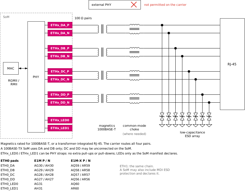
(informative): ETHx carrier chain: on-module PHY, MDI pads, 100 Ω differential pairs, magnetics rated for 1000BASE-T, common-mode choke where needed, low-capacitance ESD array and RJ-45.
| E1M-X coord(s) | E1M coord(s) | Pin name |
|---|---|---|
| AR59 | AH30 | ETH0_DA_N |
| AQ59 | AG30 | ETH0_DA_P |
| AR58 | AH29 | ETH0_DB_N |
| AQ58 | AG29 | ETH0_DB_P |
| AR57 | AH28 | ETH0_DC_N |
| AQ57 | AG28 | ETH0_DC_P |
| AR56 | AH27 | ETH0_DD_N |
| AQ56 | AG27 | ETH0_DD_P |
| AQ60 | AG31 | ETH0_LED0 |
| AR60 | AH31 | ETH0_LED1 |
| AR52 | AH23 | ETH1_DA_N |
| AQ52 | AG23 | ETH1_DA_P |
| AR51 | AH22 | ETH1_DB_N |
| AQ51 | AG22 | ETH1_DB_P |
| AR50 | AH21 | ETH1_DC_N |
| AQ50 | AG21 | ETH1_DC_P |
| AR49 | AH20 | ETH1_DD_N |
| AQ49 | AG20 | ETH1_DD_P |
| AQ53 | AG24 | ETH1_LED0 |
| AR53 | AH24 | ETH1_LED1 |
7.3.7 PCIe
E1M provides one × 4 PCIe controller; E1M-X provides two.
| E1M-X coord(s) | E1M coord(s) | Pin name |
|---|---|---|
| B47 | B29 | PCIE0_CLK_N |
| A47 | A29 | PCIE0_CLK_P |
| B42 | B25 | PCIE0_RX0_N |
| A42 | A25 | PCIE0_RX0_P |
| B43 | B26 | PCIE0_RX1_N |
| A43 | A26 | PCIE0_RX1_P |
| B44 | B27 | PCIE0_RX2_N |
| A44 | A27 | PCIE0_RX2_P |
| B45 | B28 | PCIE0_RX3_N |
| A45 | A28 | PCIE0_RX3_P |
| B38 | B21 | PCIE0_TX0_N |
| A38 | A21 | PCIE0_TX0_P |
| B39 | B22 | PCIE0_TX1_N |
| A39 | A22 | PCIE0_TX1_P |
| B40 | B23 | PCIE0_TX2_N |
| A40 | A23 | PCIE0_TX2_P |
| B41 | B24 | PCIE0_TX3_N |
| A41 | A24 | PCIE0_TX3_P |
| B36 | (E1M-X only) | PCIE1_CLK_N |
| A36 | (E1M-X only) | PCIE1_CLK_P |
| B31 | (E1M-X only) | PCIE1_RX0_N |
| A31 | (E1M-X only) | PCIE1_RX0_P |
| B32 | (E1M-X only) | PCIE1_RX1_N |
| A32 | (E1M-X only) | PCIE1_RX1_P |
| B33 | (E1M-X only) | PCIE1_RX2_N |
| A33 | (E1M-X only) | PCIE1_RX2_P |
| B34 | (E1M-X only) | PCIE1_RX3_N |
| A34 | (E1M-X only) | PCIE1_RX3_P |
| B27 | (E1M-X only) | PCIE1_TX0_N |
| A27 | (E1M-X only) | PCIE1_TX0_P |
| B28 | (E1M-X only) | PCIE1_TX1_N |
| A28 | (E1M-X only) | PCIE1_TX1_P |
| B29 | (E1M-X only) | PCIE1_TX2_N |
| A29 | (E1M-X only) | PCIE1_TX2_P |
| B30 | (E1M-X only) | PCIE1_TX3_N |
| A30 | (E1M-X only) | PCIE1_TX3_P |
7.3.8 I2C
| E1M-X coord(s) | E1M coord(s) | Pin name |
|---|---|---|
| AH1 | AE2 | I2C0_SCL |
| AH2 | AD2 | I2C0_SDA |
| AQ47 | AG17 | I2C1_SCL |
| AR47 | AH17 | I2C1_SDA |
| E64 | (E1M-X only) | I2C2_SCL |
| E63 | (E1M-X only) | I2C2_SDA |
| A24 | (E1M-X only) | I2C3_SCL |
| A23 | (E1M-X only) | I2C3_SDA |
7.3.9 I3C
| E1M-X coord(s) | E1M coord(s) | Pin name |
|---|---|---|
| AQ19 | AG5 | I3C_SCL |
| AR19 | AH5 | I3C_SDA |
7.3.10 UART
This revision specifies only the data lines (TX/RX) of each UART. Carrier-board flow control via RTS/CTS is permitted via the silicon-specific alt-function policy (§8.4) but is not part of default-function conformance.
Both form factors expose a dedicated debug-console UART on DBG_TX / DBG_RX. It is intended for the SoM's boot/console output and is not counted among the general-purpose UARTs in §7.2. DBG_TX is a SoM output and DBG_RX a SoM input, both in the VIO_OUT domain; the carrier SHALL drive DBG_RX only while VIO_OUT is high (§6.2.3). Carriers SHOULD bring DBG_TX / DBG_RX to a header or to a USB-to-UART bridge referenced to VIO_OUT. The SoM SHALL declare the console's role and settings in its manifest. Informative: on E1M-AEN, DBG_TX / DBG_RX are the Alif Secure Enclave UART.
| E1M-X coord(s) | E1M coord(s) | Pin name |
|---|---|---|
| AD62 | AE3 | DBG_RX |
| AC62 | AD3 | DBG_TX |
| AB2 | G2 | UART0_RX |
| AA2 | F2 | UART0_TX |
| AR17 | AH4 | UART1_RX |
| AQ17 | AG4 | UART1_TX |
7.3.11 SPI
| E1M-X coord(s) | E1M coord(s) | Pin name |
|---|---|---|
| AE1 | M1 | SPI0_CS0 |
| AF1 | N1 | SPI0_CS1 |
| AD1 | L1 | SPI0_MISO |
| AD2 | M2 | SPI0_MOSI |
| AE2 | N2 | SPI0_SCLK |
| AR14 | AH9 | SPI1_CS0 |
| AR13 | AH8 | SPI1_CS1 |
| AQ13 | AG8 | SPI1_MISO |
| AQ14 | AG9 | SPI1_MOSI |
| AR15 | AG10 | SPI1_SCLK |
| C64 | (E1M-X only) | SPI2_CS0 |
| D64 | (E1M-X only) | SPI2_CS1 |
| B63 | (E1M-X only) | SPI2_MISO |
| B64 | (E1M-X only) | SPI2_MOSI |
| C63 | (E1M-X only) | SPI2_SCLK |
7.3.12 I2S
| E1M-X coord(s) | E1M coord(s) | Pin name |
|---|---|---|
| AQ5 | AE33 | I2S0_SCLK |
| AQ4 | AD33 | I2S0_SDI |
| AR4 | AD34 | I2S0_SDO |
| AR5 | AE34 | I2S0_WS |
| AR11 | AH7 | I2S1_SCLK |
| AR10 | AH6 | I2S1_SDI |
| AQ10 | AG6 | I2S1_SDO |
| AQ11 | AG7 | I2S1_WS |
7.3.13 SWD / JTAG
Two pads carry compound primary functions; either name in the slash combo is conformant. Selection is a carrier-board decision (§8.3).
| E1M-X coord(s) | E1M coord(s) | Pin name |
|---|---|---|
| AJ1 | X1 | JTAG_TCK/SWDCLK |
| AJ2 | X2 | JTAG_TDI |
| AK2 | Y2 | JTAG_TDO |
| AK1 | Y1 | JTAG_TMS/SWDIO |
| AL1 | Z1 | JTAG_nRST |
7.3.14 CAN bus
Each CAN group (CAN0, and on E1M-X also CAN1) is implemented in one of the two options of §6.5, declared for each group in the per-SoM manifest. The slash-combo silkscreen names both readings:
- Bus-level CAN.
CANxH/CANx_TXcarriesCANxHandCANxL/CANx_RXcarriesCANxLfrom an on-module transceiver. The carrier provides termination, bus-side ESD protection and the connector, and SHALL NOT add a transceiver. - Logic-level CAN.
CANxH/CANx_TXcarries the controller outputCANx_TXandCANxL/CANx_RXcarries the controller inputCANx_RX, both in theVIO_OUT(1.8 V) domain. The carrier SHALL provide a CAN transceiver whose logic-side supply isVIO_OUT(or a carrier rail switched byVIO_OUT, §6.1.2) and whose logic pins are high-impedance while it is unpowered, plus termination, bus-side ESD protection and the connector.
A carrier SHALL NOT connect a CAN bus, a bus terminator or bus-side protection directly to a CAN pad unless every SoM it declares support for implements that CAN group as bus-level CAN. A carrier that supports both options SHALL follow §6.7.2; its default assembly is the carrier-transceiver path.
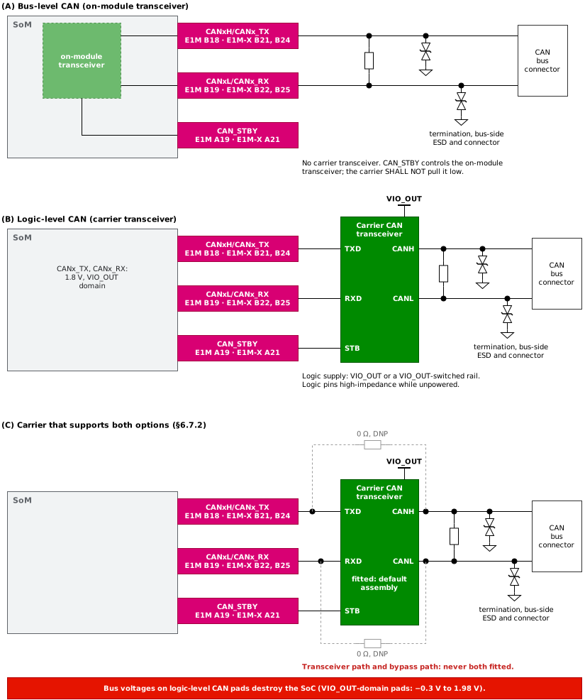
(informative): CAN options. (A) bus-level CAN; (B) logic-level CAN with a carrier transceiver; (C) a carrier that supports both options, with the carrier-transceiver path as the default assembly (§6.7.2).
CAN_STBY is the standby control of the CAN transceiver. On a bus-level group it controls the on-module transceiver; on a logic-level group the SoM MAY use it to drive the standby input of the carrier transceiver. The SoM SHALL declare the direction and polarity of CAN_STBY in its manifest. The carrier SHALL NOT pull CAN_STBY low, and SHALL NOT drive it unless the SoM manifest declares it a SoM input. Informative: on the E1M-AEN transceiver assembly option, CAN_STBY (A19) is the TI TCAN1044AVDRBRQ1 standby input (low = normal mode); on the E1M-AEN standard build it is a SoC GPIO.
| E1M-X coord(s) | E1M coord(s) | Pin name |
|---|---|---|
| B21 | B18 | CAN0H/CAN0_TX |
| B22 | B19 | CAN0L/CAN0_RX |
| B24 | (E1M-X only) | CAN1H/CAN1_TX |
| B25 | (E1M-X only) | CAN1L/CAN1_RX |
| A21 | A19 | CAN_STBY |
7.3.15 SDIO / SD card
| E1M-X coord(s) | E1M coord(s) | Pin name |
|---|---|---|
| AQ31 | AG11 | SD_CLK |
| AR31 | AH11 | SD_CMD |
| AQ32 | AG12 | SD_D0 |
| AR33 | AH13 | SD_D1 |
| AQ33 | AG13 | SD_D2 |
| AR34 | AH14 | SD_D3 |
| AQ34 | AG14 | SD_DET |
| AR32 | AH12 | SD_RST |
| AQ30 | AH10 | SD_VDD_OUT (E1M-X) / SD_VDD (E1M) |
7.3.16 MIPI DSI display
E1M and E1M-X each provide two 4-lane MIPI DSI interfaces (DSI0, DSI1). Backlight control pads are listed in §7.3.1.
| E1M-X coord(s) | E1M coord(s) | Pin name |
|---|---|---|
| B61 | F34 | DSI0_0_N |
| A61 | F33 | DSI0_0_P |
| B60 | E34 | DSI0_1_N |
| A60 | E33 | DSI0_1_P |
| B59 | C34 | DSI0_2_N |
| A59 | C33 | DSI0_2_P |
| B58 | B34 | DSI0_3_N |
| A58 | B33 | DSI0_3_P |
| B57 | D34 | DSI0_C_N |
| A57 | D33 | DSI0_C_P |
| B53 | L34 | DSI1_0_N |
| A53 | L33 | DSI1_0_P |
| B52 | K34 | DSI1_1_N |
| A52 | K33 | DSI1_1_P |
| B51 | I34 | DSI1_2_N |
| A51 | I33 | DSI1_2_P |
| B50 | H34 | DSI1_3_N |
| A50 | H33 | DSI1_3_P |
| B49 | J34 | DSI1_C_N |
| A49 | J33 | DSI1_C_P |
7.3.17 MIPI CSI camera
E1M provides two 4-lane MIPI CSI-2 interfaces; E1M-X provides four. Per-camera LDO outputs (+V_CAM*, CAM_VFB*) are listed in §7.3.1.
| E1M-X coord(s) | E1M coord(s) | Pin name |
|---|---|---|
| T64 | R34 | CSI0_0_N |
| T63 | R33 | CSI0_0_P |
| S64 | Q34 | CSI0_1_N |
| S63 | Q33 | CSI0_1_P |
| Q64 | O34 | CSI0_2_N |
| Q63 | O33 | CSI0_2_P |
| P64 | N34 | CSI0_3_N |
| P63 | N33 | CSI0_3_P |
| R64 | P34 | CSI0_C_N |
| R63 | P33 | CSI0_C_P |
| Z64 | X34 | CSI1_0_N |
| Z63 | X33 | CSI1_0_P |
| Y64 | W34 | CSI1_1_N |
| Y63 | W33 | CSI1_1_P |
| W64 | U34 | CSI1_2_N |
| W63 | U33 | CSI1_2_P |
| V64 | T34 | CSI1_3_N |
| V63 | T33 | CSI1_3_P |
| X64 | V34 | CSI1_C_N |
| X63 | V33 | CSI1_C_P |
| AF64 | (E1M-X only) | CSI2_0_N |
| AF63 | (E1M-X only) | CSI2_0_P |
| AE64 | (E1M-X only) | CSI2_1_N |
| AE63 | (E1M-X only) | CSI2_1_P |
| AC64 | (E1M-X only) | CSI2_2_N |
| AC63 | (E1M-X only) | CSI2_2_P |
| AB64 | (E1M-X only) | CSI2_3_N |
| AB63 | (E1M-X only) | CSI2_3_P |
| AD64 | (E1M-X only) | CSI2_C_N |
| AD63 | (E1M-X only) | CSI2_C_P |
| AL64 | (E1M-X only) | CSI3_0_N |
| AL63 | (E1M-X only) | CSI3_0_P |
| AK64 | (E1M-X only) | CSI3_1_N |
| AK63 | (E1M-X only) | CSI3_1_P |
| AI64 | (E1M-X only) | CSI3_2_N |
| AI63 | (E1M-X only) | CSI3_2_P |
| AH64 | (E1M-X only) | CSI3_3_N |
| AH63 | (E1M-X only) | CSI3_3_P |
| AJ64 | (E1M-X only) | CSI3_C_N |
| AJ63 | (E1M-X only) | CSI3_C_P |
7.3.18 Parallel camera
E1M exposes 8 parallel-camera data lines (CAM_D1–CAM_D8). E1M-X exposes 16 (CAM_D1–CAM_D16).
| E1M-X coord(s) | E1M coord(s) | Pin name |
|---|---|---|
| G62 | W32 | CAM_D1 |
| H62 | X32 | CAM_D2 |
| I62 | Y32 | CAM_D3 |
| J62 | Z32 | CAM_D4 |
| K62 | AA32 | CAM_D5 |
| L62 | AB32 | CAM_D6 |
| M62 | AC32 | CAM_D7 |
| N62 | AD32 | CAM_D8 |
| O62 | (E1M-X only) | CAM_D9 |
| P62 | (E1M-X only) | CAM_D10 |
| Q62 | (E1M-X only) | CAM_D11 |
| R62 | (E1M-X only) | CAM_D12 |
| S62 | (E1M-X only) | CAM_D13 |
| T62 | (E1M-X only) | CAM_D14 |
| U62 | (E1M-X only) | CAM_D15 |
| V62 | (E1M-X only) | CAM_D16 |
| C62 | T32 | CAM_HSYNC |
| E62 | V32 | CAM_PCLK |
| D62 | S32 | CAM_VSYNC |
| F62 | U32 | CAM_XVCLK |
7.3.19 LCD parallel display
E1M-X exposes a 24-bit RGB parallel LCD interface plus H/V sync. This interface is not present on E1M.
| E1M-X coord(s) | E1M coord(s) | Pin name |
|---|---|---|
| D3 | (E1M-X only) | LCD_B0 |
| E3 | (E1M-X only) | LCD_B1 |
| F3 | (E1M-X only) | LCD_B2 |
| G3 | (E1M-X only) | LCD_B3 |
| H3 | (E1M-X only) | LCD_B4 |
| I3 | (E1M-X only) | LCD_B5 |
| J3 | (E1M-X only) | LCD_B6 |
| K3 | (E1M-X only) | LCD_B7 |
| L3 | (E1M-X only) | LCD_B8 |
| M3 | (E1M-X only) | LCD_B9 |
| N3 | (E1M-X only) | LCD_B10 |
| O3 | (E1M-X only) | LCD_B11 |
| P3 | (E1M-X only) | LCD_B12 |
| Q3 | (E1M-X only) | LCD_B13 |
| R3 | (E1M-X only) | LCD_B14 |
| S3 | (E1M-X only) | LCD_B15 |
| T3 | (E1M-X only) | LCD_B16 |
| U3 | (E1M-X only) | LCD_B17 |
| V3 | (E1M-X only) | LCD_B18 |
| W3 | (E1M-X only) | LCD_B19 |
| X3 | (E1M-X only) | LCD_B20 |
| Y3 | (E1M-X only) | LCD_B21 |
| Z3 | (E1M-X only) | LCD_B22 |
| AA3 | (E1M-X only) | LCD_B23 |
| AB3 | (E1M-X only) | LCD_HSYNC |
| AC3 | (E1M-X only) | LCD_VSYNC |
7.3.20 PDM microphone
| E1M-X coord(s) | E1M coord(s) | Pin name |
|---|---|---|
| AQ7 | AA1 | PDM_C0 |
| AQ8 | AB1 | PDM_C1 |
| AR7 | AA2 | PDM_D0 |
| AR8 | AB2 | PDM_D1 |
7.3.21 Analogue inputs (ADC)
| E1M-X coord(s) | E1M coord(s) | Pin name |
|---|---|---|
| A17 | A15 | ANA_S0 |
| B17 | B15 | ANA_S1 |
| A16 | A14 | ANA_S2 |
| B16 | B14 | ANA_S3 |
| A15 | A13 | ANA_S4 |
| B15 | B13 | ANA_S5 |
| A14 | A12 | ANA_S6 |
| B14 | B12 | ANA_S7 |
7.3.22 Analogue outputs (DAC)
| E1M-X coord(s) | E1M coord(s) | Pin name |
|---|---|---|
| A19 | A16 | DAC0 |
| B19 | B16 | DAC1 |
7.3.23 Quadrature encoder
| E1M-X coord(s) | E1M coord(s) | Pin name |
|---|---|---|
| A12 | A10 | ENC0_X |
| B12 | B10 | ENC0_Y |
| A11 | A9 | ENC1_X |
| B11 | B9 | ENC1_Y |
| A10 | A8 | ENC2_X |
| B10 | B8 | ENC2_Y |
| A9 | A7 | ENC3_X |
| B9 | B7 | ENC3_Y |
7.3.24 PWM
| E1M-X coord(s) | E1M coord(s) | Pin name |
|---|---|---|
| A7 | A6 | PWM0 |
| B7 | B6 | PWM1 |
| A6 | A5 | PWM2 |
| B6 | B5 | PWM3 |
| A5 | A4 | PWM4 |
| B5 | B4 | PWM5 |
| A4 | A3 | PWM6 |
| B4 | B3 | PWM7 |
7.3.25 GPIO
The pads listed below have GPIO as their default function. Per §8.2, every other digital pad MAY also be repurposed as GPIO (secondary), but those are not enumerated here.
| E1M-X coord(s) | E1M coord(s) | Pin name |
|---|---|---|
| L2 | L2 | IO0 |
| M2 | (E1M-X only) | IO1 |
| N2 | W2 | IO2 |
| O2 | AG2 | IO3 |
| AF2 | AG16 | IO4 |
| AG2 | AH18 | IO5 |
| AL2 | AG18 | IO6 |
| (E1M only) | AG34 | IO7 |
| AR21 | AG33 | IO8 |
| AQ21 | AH34 | IO9 |
| AR22 | AH33 | IO10 |
| AQ22 | A18 | IO11 |
| AR23 | (E1M-X only) | IO12 |
| AQ23 | E3 | IO13 |
| AR24 | (E1M-X only) | IO14 |
| AQ24 | F3 | IO15 |
| AR25 | G3 | IO16 |
| AQ26 | H3 | IO17 |
| AR26 | I3 | IO18 |
| AQ27 | J3 | IO19 |
| AR27 | K3 | IO20 |
| AQ28 | L3 | IO21 |
| AR28 | M3 | IO22 |
| (E1M only) | N3 | IO23 |
| AR29 | O3 | IO24 |
| F63 | P3 | IO25 |
| F64 | (E1M-X only) | IO26 |
| AN63 | (E1M-X only) | IO27 |
| AN64 | (E1M-X only) | IO28 |
| AO63 | (E1M-X only) | IO29 |
| AO64 | (E1M-X only) | IO30 |
| AP63 | (E1M-X only) | IO31 |
| AP64 | (E1M-X only) | IO32 |
| AQ63 | (E1M-X only) | IO33 |
| AQ64 | (E1M-X only) | IO34 |
| A25 | (E1M-X only) | IO35 |
8 Alternative-function policy
8.1 Default function
Every E1M pad has exactly one default primary function fixed by this specification. The default function SHALL match the default field of the corresponding pad in pinout/v1.json or pinout/x-v1.json, which in turn matches the Pin name column of §7.3.
Conformant SoMs SHALL route the default function to the named pad on every pad they expose. SoMs MAY leave any pad unconnected; an unconnected pad SHALL NOT appear in the per-SoM manifest's routes list (it MAY appear in not_routed).
8.2 GPIO secondary
For any pad whose default function is a digital signal — that is, not in the set { GND, NC, RSVD, POWER_*, ANT_*, BL_LED_A, BL_LED_K } — a conformant SoM MAY additionally expose the pad as a general-purpose digital I/O (GPIO).
A carrier board that uses a pad as GPIO SHALL remain hardware-compatible with any conformant SoM that routes only the default function on that pad, provided the carrier board treats the pad as default-driven when no GPIO software is loaded.
In the JSON, the GPIO secondary is expressed by including { "signal": "GPIO" } in the pad's alt array.
Pad IO25 (E1M P3, E1M-X F63) additionally defines the alternate function RTC_WAKE_N: an active-low, open-drain RTC wake / interrupt output from the module. A SoM that exposes it SHALL drive it open-drain from its always-on domain, keep it valid in every power state while VDD_5V_IN is present, and tolerate up to 5.5 V on the pad (5 V tolerant). The carrier supplies the pull-up, to its own or the host's always-on rail; RTC_WAKE_N is an exception to §6.2.3 clauses 1 and 4. The JSON expresses it as { "signal": "RTC_WAKE_N" } in the pad's alt array.
8.3 Compound-function pins
Some pads carry two equally-conformant primary functions. The silkscreen for such a pad uses a slash to combine the two names. The JSON encodes the first name as default and the second name as the first entry of alt, ahead of the GPIO secondary. Compound pins present in this revision:
JTAG_TCK/SWDCLK,JTAG_TMS/SWDIOCAN0H/CAN0_TX,CAN0L/CAN0_RX,CAN1H/CAN1_TX,CAN1L/CAN1_RX
Both functions of a compound pad are conformant. For the JTAG / SWD compound pads, carrier boards MAY select either function; selection is a per-board decision. For the CAN compound pads, the reading is fixed by the CAN option the SoM declares for that group (§6.5, §7.3.14), and the carrier SHALL use the declared reading.
8.4 Per-SoM tertiary functions
Functions beyond the default and the GPIO secondary (and, where applicable, the second name of a compound pin) are silicon-specific. Such tertiary functions SHALL NOT be assumed by carrier boards that target the standard generically. A carrier board that requires a tertiary function SHALL declare a per-SoM dependency in its build system and reject any SoM whose manifest does not expose that function.
The set of tertiary functions a SoM exposes SHALL be declared in its per-SoM manifest (Annex C).
8.5 Peripheral-instance naming
Where a pad belongs to a multi-instance peripheral (multiple I2C controllers, multiple PCIe controllers, etc.), the JSON pad records the instance in its instance field. Instance names MUST match the pattern:
^(I2C|I3C|SPI|UART|I2S|CSI|DSI|LCD|PWM|ADC|DAC|USB|ETH|PCIE|CAN|SDIO|JTAG|PDM|ENC|PARCAM|BL|CAM|BOOT)\d*$
Pads without a peripheral context (e.g. GND, VDD_5V_IN, antenna outputs) MAY omit the instance field.
9 Conformance
9.1 SoM conformance
A System-on-Module is E1M-conformant if and only if every clause below is satisfied for the form factor it declares (E1M or E1M-X):
- Mechanical. The outline matches the form-factor envelope per §4 and §5, within the tolerances specified.
- Pinout. For every pad the SoM routes, the pad's BGA coordinate and
defaultsignal class match the corresponding entry inpinout/v1.json(E1M) orpinout/x-v1.json(E1M-X). The SoM MAY leave any pad as no-connect. - Electrical. The SoM meets the SoM-side clauses of §6.1.1 (clause 9), §6.1.2, §6.2, §6.3 and §6.3.1. The remaining absolute maximum ratings and recommended operating conditions of §6.6 are TBD in this revision.
- Boot. The SoM exposes
BOOT0–BOOT3on its footprint at the pad locations of §7.3.1, per §6.4. The per-SoM manifest declares the strap mapping, or declares that the SoM ignores the strap (§6.4 (3)); a SoM that ignores the strap and declares it is conformant. - Mandatory on-module components. The SoM integrates an on-module Ethernet PHY for every Ethernet group it exposes, an on-module Wi-Fi 6 + BLE 5.4 combo radio with 2.4 GHz operation (5 GHz and 6 GHz optional and declared), and, for every CAN group it exposes, either an on-module CAN transceiver or the declared logic-level CAN option — per §6.5.
- Manifest. The SoM publishes a per-SoM manifest conforming to the format in Annex C, including every declaration that §6 and §7 require: 5 V input values (§6.1.1),
VIO_OUTlimits (§6.1.2), power-up delay (§6.2.1), switched pad groups (§6.2.3), standby protocol and minimum reset pulse (§6.3.1), boot-strap mapping or ignored strap (§6.4), Wi-Fi bands and unused antenna pads (§6.5, §7.3.2), pads outside theVIO_OUTdomain (§6.7.1), Ethernet link rate and MDI ESD (§7.3.6), debug console (§7.3.10), and CAN option andCAN_STBYdirection (§7.3.14).
9.2 Carrier-board conformance
A carrier board is E1M-conformant if all of the following hold:
- The mating land pattern, power delivery, and pad-by-pad signal usage match the chosen form factor's coordinate space.
- The carrier does not require any tertiary function (§8.4) unless it explicitly targets a single SoM or set of SoMs (declared in the carrier's BOM / build system).
- The carrier connects every
GNDpad of the SoM to a low-impedance ground plane. - 5 V input. The carrier meets §6.1.1 clauses 1–8.
VIO_OUT. The carrier meets §6.1.2 clauses 2–6.- Sequencing and back-powering. The carrier meets §6.2.1, §6.2.2 and §6.2.3.
- Control pads. The carrier drives
MODULE_EN,MODULE_STBY,PORnandJTAG_nRSTper §6.3.1. - Pad domains and default fits. The carrier meets §6.7.1 and §6.7.2, and declares, for every build variant, the fit of each dual-meaning pad group and the SoMs it supports.
- Reserved and not-routed pads. The carrier leaves every
RSVDpad unconnected (§7.3.3) and routes no unrelated net through a pad that a SoM does not route (§7.3.4). - Interfaces. The carrier meets the carrier clauses of §7.3.6 (Ethernet), §7.3.10 (debug UART) and §7.3.14 (CAN).
- Mounting. The SoM is not placed directly on the carrier: the carrier uses a spacer PCB soldered on both faces (§5.2 option (a)) or a through-cutout of the size and position given in §5.2 option (b), and under either option carries no components inside the cavity outline.
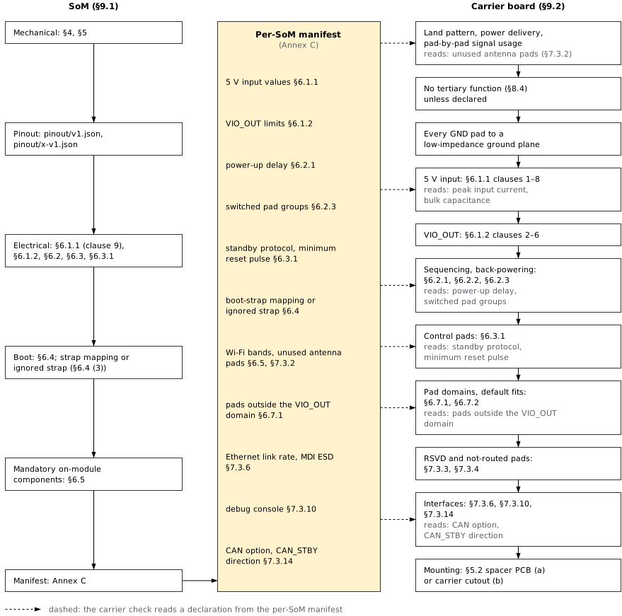
(informative): SoM and carrier-board conformance checks (§9.1, §9.2) and the manifest declarations that the carrier checks read.
9.3 Optional vs. mandatory pad classes
This revision does not partition pads into mandatory vs. optional classes. A future minor release SHOULD define:
- Mandatory pads —
GND,VDD_5V_IN,MODULE_EN,PORn,BOOT0–BOOT3(which a SoM MAY ignore as §6.4 (3) permits),JTAG_*. - Optional pads — All other interface pads.
Until that partitioning is published, conformant SoMs MAY omit any non-power, non-reserved, non-debug pad without losing conformance.
10 Trademarks, licensing, and intellectual property
10.1 Trademarks
"E1M™" and "Edge-1 AI Module™" are trademarks of Alp Lab AB. Products that conform to this specification MAY NOT use these trademarks without separate written permission from Alp Lab AB. Implementations MAY truthfully describe themselves as "E1M-compatible" or "implementing the E1M v1.0 specification" without using the trademarks.
10.2 Licensing of this specification
This specification (the prose, the pinout JSONs, the JSON Schema, the example manifests, and the Altium pin-list exports under source/) is licensed under the Creative Commons Attribution-ShareAlike 4.0 International License (CC BY-SA 4.0). See LICENSE for the full notice.
10.3 What is not licensed under CC BY-SA 4.0
The proprietary System-on-Module designs that implement this specification — including but not limited to ALP-AEN, ALP-X-V2N, ALP-X-V2N-M1, their schematics, PCB layouts, Altium libraries, BOMs, manufacturing files, firmware, and software — are not part of this repository and are not licensed under CC BY-SA 4.0. Those artefacts are proprietary to Alp Lab AB and require a separate written agreement.
10.4 Disclaimers
Alp Lab AB provides this specification "AS IS" and disclaims all warranties of merchantability or fitness for any particular purpose. Compliance with this specification does not absolve manufacturers from the requirements of safety and regulatory agencies (EN, UL, CSA, FCC, IEC, etc.). All content and information within this document are subject to change without prior notice.
11 Annex A (informative) — Reference SoM constructions
This annex describes on-module components used by the rev 1.0 reference SoMs. The information is informative; conformant SoMs MAY use any component set that satisfies §4–§9.
| Reference SoM family | Form factor | Primary silicon | SKUs | Detail |
|---|---|---|---|---|
| E1M-AEN | E1M | Alif Semiconductor Ensemble (E3– E8) | E1M-AEN301, E1M-AEN401, E1M-AEN501, E1M-AEN601, E1M-AEN701, E1M-AEN801, E1M-AEN803 | §A.1 |
| E1M-X V2N | E1M-X | Renesas RZ/V2N (CA55 + CM33 + DRP-AI3) | E1M-V2N101, E1M-V2N102, E1M-V2N103 | §A.2 |
| E1M-X V2N-M1 | E1M-X | Renesas RZ/V2N + DeepX DX-M1 | E1M-V2M101, E1M-V2M102, E1M-V2M103 | §A.3 |
11.1 E1M-AEN family (seven SKUs, shared E1M routing)
The E1M-AEN family pairs the Alif Semiconductor Ensemble SoC family with the E1M (35 × 35 mm) form factor. All seven SKUs use the same package routing, the same on-module PMIC, the same Wi-Fi 6 + BLE 5.4 combo (TI CC3501E) and the same 100 Mbps Ethernet PHY (TI DP83825). The standard build has no on-module CAN transceiver: B18 / B19 carry CAN0_TX / CAN0_RX as 1.8 V SoC logic, A19 (CAN_STBY) is a SoC GPIO, and the manifest declares the logic-level CAN option (§6.5, §7.3.14). An on-module TI TCAN1044AVDRBRQ1 transceiver is an assembly option; with it fitted, B18 / B19 carry CAN0H / CAN0L (bus-level CAN) and A19 is the transceiver standby input. They differ only in SoC choice (Ensemble variant), internal RAM size, optional ISP / JPEG-encoder presence, and on-module OSPI memory population: E1M-AEN803 is the E1M-AEN801 silicon and PCB with both external OSPI memories fitted (512 Mbit HyperRAM + 256 Mbit NOR flash).
| SKU | Variant | Alif part number | App CPU | Real-time CPU | NPU | ISP / JPEG |
|---|---|---|---|---|---|---|
E1M-AEN301 | E3 | AE302F80F55D5LE | — | 1 × M55 @ 160 MHz + 1 × M55 @ 400 MHz | 2 × Ethos-U55 (1 × 46 GOPS + 1 × 204 GOPS) | — |
E1M-AEN401 | E4 | AE402FA0E5597LE0 | — | 1 × M55 @ 160 MHz + 1 × M55 @ 400 MHz | 2 × Ethos-U55 + 1 × Ethos-U85 (1 × 46 GOPS + 2 × 204 GOPS) | ISP + JPEG encoder |
E1M-AEN501 | E5 | AE512F80F55D5LS | 1 × Cortex-A32 @ 800 MHz | 1 × M55 @ 160 MHz + 1 × M55 @ 400 MHz | 2 × Ethos-U55 (1 × 46 GOPS + 1 × 204 GOPS) | — |
E1M-AEN601 | E6 | AE612FA0E5597LS0 | 1 × Cortex-A32 @ 800 MHz | 1 × M55 @ 160 MHz + 1 × M55 @ 400 MHz | 2 × Ethos-U55 + 1 × Ethos-U85 (1 × 46 GOPS + 2 × 204 GOPS) | ISP + JPEG encoder |
E1M-AEN701 | E7 | AE722F80F55D5LS | 2 × Cortex-A32 @ 800 MHz | 1 × M55 @ 160 MHz + 1 × M55 @ 400 MHz | 2 × Ethos-U55 (1 × 46 GOPS + 1 × 204 GOPS) | — |
E1M-AEN801 | E8 | AE822FA0E5597LS0 | 2 × Cortex-A32 @ 800 MHz | 1 × M55 @ 160 MHz + 1 × M55 @ 400 MHz | 2 × Ethos-U55 + 1 × Ethos-U85 (1 × 46 GOPS + 2 × 204 GOPS) | ISP + JPEG encoder |
E1M-AEN803 | E8 | AE822FA0E5597LS0 | 2 × Cortex-A32 @ 800 MHz | 1 × M55 @ 160 MHz + 1 × M55 @ 400 MHz | 2 × Ethos-U55 + 1 × Ethos-U85 (1 × 46 GOPS + 2 × 204 GOPS) | ISP + JPEG encoder |
All seven SKUs are RoHS and rated for operating temperature − 40 to +75 °C. The E3, E5 and E7 SKUs use Alif AE…F80F55D5L… parts and the E4, E6 and E8 SKUs Alif AE…FA0E5597L…0 parts (part numbers above).
Every E1M-AEN SKU routes the same subset of the E1M pads. Notably:
- Ethernet: only
ETH0_*is routed (Ensemble has one MAC). - MIPI CSI-2: only
CSI0_*is routed (one camera, 2 lanes). - MIPI DSI: only
DSI0_*is routed (one display, 2 lanes). - PCIe: not routed.
- CAN:
CAN0only; logic-level CAN on the standard build (see above). - Debug UART:
DBG_TX/DBG_RX(AD3/AE3) carry the Alif Secure Enclave UART. - USB: USB 2.0 only (
USB2_*). - Wi-Fi: 2.4 GHz only, on
ANT_2.4GHZ(AH1).ANT_5GHZ(AF1) andANT_6GHZ(AD1) are NC; the manifest declares the 2.4 GHz band and the two unused antenna pads (§6.5, §7.3.2). - Boot strap:
BOOT0–BOOT3are not routed; the AEN family does not support strap-driven boot mode selection. Pads are NC, and the manifest declares the strap ignored (§6.4 (3)). - Standby:
MODULE_STBYenters real-time-clock standby only.
Memory per SKU (DS-AEN-001): 5.5 MB internal MRAM on every SKU; internal RAM 13.5 MB (E3, E5, E7) or 9.75 MB (E4, E6, E8). External OSPI memory: E1M-AEN803 fits 512 Mbit HyperRAM + 256 Mbit NOR flash, E1M-AEN801 fits none, and E1M-AEN301 / 401 / 501 / 601 / 701 have on-die memory only in the standard build (external memory is an assembly option). Details are in the ALP-AEN Hardware Design Guide and the ALP-AEN Datasheet, both maintained outside this repository.
11.2 E1M-X V2N family (Renesas RZ/V2N)
The E1M-X V2N family pairs the Renesas RZ/V2N vision-AI MPU with the E1M-X (45 × 65 mm) form factor. Three SKUs differ only in memory tier:
| SKU | Renesas part | LPDDR4X | eMMC |
|---|---|---|---|
E1M-V2N101 | R9A09G056N44GBG#AC0 | 4 GB | eMMC 5.1, 4 GB |
E1M-V2N102 | R9A09G056N44GBG#AC0 | 8 GB | eMMC 5.1, 16 GB |
E1M-V2N103 | R9A09G056N44GBG#AC0 | 4 GB | eMMC 5.1, 16 GB |
Common silicon and capability across all three SKUs:
| Item | Value |
|---|---|
| Application CPU | 4 × Arm Cortex-A55 @ 1.8 GHz |
| Real-time CPU | Arm Cortex-M33 @ 200 MHz |
| Dedicated I/O MCU | Arm Cortex-M33 @ 216 MHz |
| AI accelerator | Renesas DRP-AI3, 4 TOPS (V2N grade) |
| ISP | Arm Mali-C55 |
| GPU | Arm Mali-G31 |
| Codec | H.264 1920 × 1080 @ 60 fps; H.265 3840 × 2160p @ 30 fps |
| MIPI DSI | 4 lanes — up to 1920 × 1200 RGB888 @ 60 fps |
| MIPI CSI | 2 × 4-lane (up to 4K @ 30 fps), 4 virtual channels |
| Wi-Fi / BLE | 2.4 / 5 / 6 GHz Wi-Fi 6 (802.11 a/b/g/n/ac/ax) + Bluetooth 5.4 |
| Ethernet | 2 × 1 Gbps PHY |
| CAN | 2 × CAN-BUS PHY |
| PCIe | PCIe 3.0 × 2 lanes |
| Boot | NOR Flash (boot-supported) |
| Operating temperature | − 40 to +85 °C |
All three SKUs additionally include an on-module display backlight driver, 4 LDOs for external cameras, NOR Flash, the I/O MCU, a TPM (secure chip), an EEPROM, an RTC, and a temperature sensor.
The supporting silicon stack is:
| Role | Part | Vendor |
|---|---|---|
| Primary MPU | R9A09G056N44GBG#AC0 | Renesas |
| Auxiliary I/O MCU | GD32G553 — Arm Cortex-M33 @ 216 MHz | GigaDevice |
| Main PMIC | ACT88760 (I2C 0x25 / 0x26) | Qorvo |
| Secondary PMIC | DA9292 (multi-channel, I2C 0x1E) | Renesas |
| Ethernet PHY (× 2) | RTL8211FI-VD-CG | Realtek |
| Wi-Fi 6 + BLE 5.4 module | LBEE5HY2FY (Type2FY, based on Infineon CYW55513) | Murata |
The GD32G553 is a separate, on-module Cortex-M33 IC, distinct from the Cortex-M33 core embedded inside the Renesas RZ/V2N. Its role is supervisory: power-rail sequencing alongside the PMIC, on-module supervisory I/O, and orchestration of the on-module peripherals during boot and low-power states. The RZ/V2N's own internal M33 (200 MHz) handles application-level real-time work and is not the same CPU as the GD32G553 (216 MHz).
11.3 E1M-X V2N-M1 family (Renesas RZ/V2N + DeepX M1)
The E1M-X V2N-M1 family is the V2N SoM with an added DeepX M1 standalone AI accelerator. Three SKUs match the V2N memory tiers:
| SKU | Renesas part | LPDDR4X | eMMC | AI capability |
|---|---|---|---|---|
E1M-V2M101 | R9A09G056N44GBG#AC0 | 4 GB | eMMC 5.1, 4 GB | V2N DRP-AI3 4 TOPS + DeepX M1 25 TOPS |
E1M-V2M102 | R9A09G056N44GBG#AC0 | 8 GB | eMMC 5.1, 16 GB | V2N DRP-AI3 4 TOPS + DeepX M1 25 TOPS |
E1M-V2M103 | R9A09G056N44GBG#AC0 | 4 GB | eMMC 5.1, 16 GB | V2N DRP-AI3 4 TOPS + DeepX M1 25 TOPS |
All other V2N attributes carry over (CPU, ISP, GPU, codec, MIPI counts, Wi-Fi / BLE, Ethernet, CAN, PCIe, plus the on-module GigaDevice GD32G553 Cortex-M33 supervisor). The DeepX M1 adds:
| Item | Value |
|---|---|
| Companion AI accelerator | DeepX DX-M1 — up to 25 TOPS |
| Companion memory | 2 × LPDDR5X |
| Companion storage | SPI NAND flash |
| Connection | DeepX M1 attached internally to the SoM via PCIe; not exposed on additional E1M-X pads |
Full silicon stack (V2N stack + DeepX M1):
| Role | Part | Vendor |
|---|---|---|
| Primary MPU | R9A09G056N44GBG#AC0 | Renesas |
| Companion AI accelerator | DX-M1 (PCIe-attached, 25 TOPS) | DeepX |
| Auxiliary I/O MCU | GD32G553 — Arm Cortex-M33 @ 216 MHz | GigaDevice |
| Main PMIC | ACT88760 (I2C 0x25 / 0x26) | Qorvo |
| Secondary PMIC | DA9292 (multi-channel, I2C 0x1E) | Renesas |
| Ethernet PHY (× 2) | RTL8211FI-VD-CG | Realtek |
| Wi-Fi 6 + BLE 5.4 module | LBEE5HY2FY (Type2FY, based on Infineon CYW55513) | Murata |
The DeepX M1 sits behind the RZ/V2N's PCIe controller, so the external-PCIe routing on PCIE0_* is effectively shared with the on-module M1. The GD32G553 supervisor is the same part used on the sibling V2N family — see §A.2 for its role.
11.4 Wireless module & antenna (E1M-X)
E1M-X may carry a Wi-Fi 6 + BLE 5.4 combo module together with an optional U.FL connector for an external antenna. The antenna may also be routed off-module to a carrier-side antenna. The antenna selection is a per-SoM choice.
11.5 Memories (E1M-X reference SoMs)
The reference E1M-X SoMs support:
- eMMC up to 256 GB.
- LPDDR4X up to 8 GB at 32-bit / 3.2 GT/s (RZ/V2N main DRAM).
- SPI NOR flash, 128 Mbit, boot-supported.
- EEPROM for board-ID / configuration storage.
- (V2N-M1 only) 2 × LPDDR5X attached to the DeepX M1.
- (V2N-M1 only) SPI NAND for the DeepX M1.
11.6 Trusted Platform Module
The rev 1.0 reference E1M-X SoMs include one Trusted Platform Module (TPM 2.0).
11.7 Real-Time Clock
E1M and E1M-X SoMs may include a battery-backed real-time clock with its 32 kHz output exposed on RTC_CLKOUT and its active-low wake / interrupt output on RTC_WAKE_N (alternate function of IO25, §8.2).
11.8 PCB temperature sensor
The reference SoMs may be assembled with an on-board PCB temperature sensor (TI TMP112D or equivalent).
12 Annex B (informative) — Loom v1 pinout JSON format
The canonical machine-readable pinouts live at:
pinout/v1.json— E1M (FC_35x35), 312 pads.pinout/x-v1.json— E1M-X (FC_45x65), 496 pads.
Both validate against pinout/schema/loom-v1.schema.json.
12.1 Top-level schema
{
  "loom_format_version": 1,
  "id": "E1M",
  "version": "1.0",
  "footprint_class": "FC_35x35",
  "outline_mm": { "w": 35, "h": 35 },
  "pads": [
    {
      "id": "A1",
      "silkscreen": "GND",
      "default": "GND",
      "alt": []
    },
    {
      "id": "X1",
      "silkscreen": "JTAG_TCK/SWDCLK",
      "default": "JTAG_TCK",
      "instance": "JTAG0",
      "alt": [
        { "signal": "SWD_CLK", "instance": "JTAG0" },
        { "signal": "GPIO" }
      ]
    }
  ]
}
12.2 Field reference
| Field | Type | Required | Description |
|---|---|---|---|
loom_format_version | integer | yes | Schema version. MUST be 1 for this revision. |
id | enum | yes | "E1M" or "E1M-X". |
version | string | yes | Form-factor revision, major.minor. |
footprint_class | enum | yes | "FC_35x35" (E1M) or "FC_45x65" (E1M-X). |
outline_mm | object | yes | { "w": <int>, "h": <int> }: the outline size. It does not set the drawing orientation; the top-view frame is given in §4.3 and §7.1. |
pads | array | yes | Array of pad objects. |
pads[].id | string | yes | BGA-style coordinate, regex ^[A-Z]+\d+$. Unique within pads. |
pads[].silkscreen | string | no | Silkscreen text from §7.3. |
pads[].default | SignalKind | yes | Primary function. |
pads[].instance | PeripheralInstance | no | Peripheral instance per §8.5. |
pads[].alt | array | yes | Alternate functions (may be empty). |
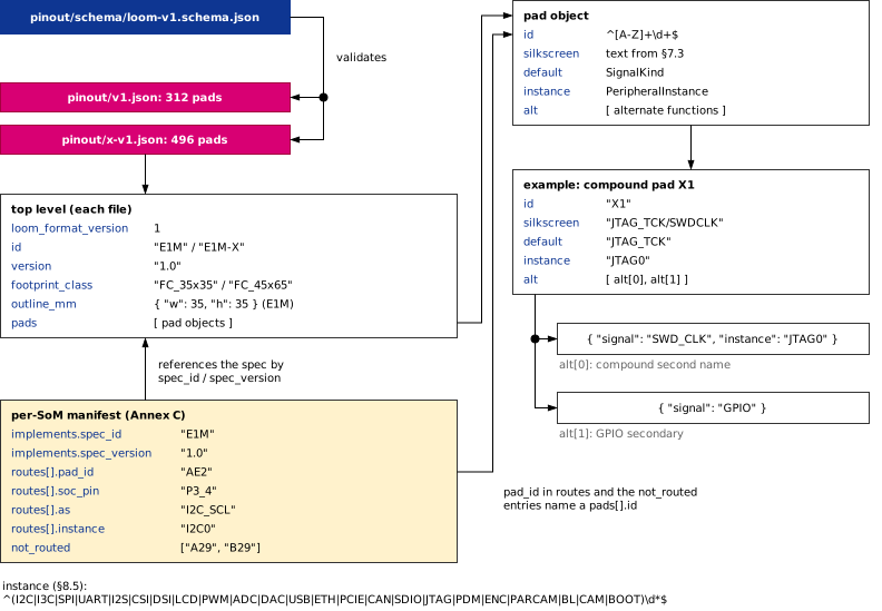
Loom v1 file structure: the top-level fields, the pad object with the compound pad X1 as an example, the schema that validates both pinout files, and the references of a per-SoM manifest (Annex C) into the specification and its pads.
12.3 SignalKind enum
The complete SignalKind enum is captured in pinout/schema/loom-v1.schema.json. Categories:
- Power & ground:
GND,POWER_5V0,POWER_3V3,POWER_1V8,POWER_VBAT,POWER_VIO_OUT,POWER_SUPER_CAP,POWER_CAM_LDO_OUT,POWER_CAM_LDO_FB,POWER_SD_VDD_OUT. - Module control:
RESET,BOOT,MODULE_EN,MODULE_STBY,RTC_CLKOUT,RTC_WAKE_N,AUDIO_CLK. - Buses:
I2C_*,I3C_*,SPI_*,UART_*,I2S_*,CAN_*,SD_*,JTAG_*,SWD_*,PDM_*,USB_*,ETH_*,PCIE_*,MIPI_CSI2_*,MIPI_DSI_*,LCD_*,PARCAM_*. - Analogue:
ADC,DAC. - Special:
ENC_X,ENC_Y,PWM,GPIO,BL_LED_A,BL_LED_K,BL_PWM,ANT_2_4GHZ,ANT_5GHZ,ANT_6GHZ,RSVD,NC.
13 Annex C (informative) — Per-SoM manifest format
Each conformant SoM publishes a manifest describing which E1M pads it routes and the silicon behind them. Manifests SHALL live in the SoM vendor's repository and reference this specification by version.
{
  "som_manifest_version": 1,
  "id": "ALP-AEN",
  "version": "0.1.0",
  "implements": {
    "spec_id": "E1M",
    "spec_version": "1.0",
    "spec_repo": "https://github.com/alplabai/e1m-spec"
  },
  "silicon": [
    {
      "role": "primary",
      "vendor": "Alif Semiconductor",
      "family": "Ensemble",
      "part": "E3"
    }
  ],
  "routes": [
    { "pad_id": "AE2", "use": "default", "soc_pin": "P3_4", "as": "I2C_SCL", "instance": "I2C0" }
  ],
  "not_routed": ["A29", "B29"],
  "electrical": {
    "vdd_5v_in": { "min_v": 4.75, "max_v": 5.25, "abs_max_v": 5.5, "ramp_max_ms": 40 },
    "vio_out": { "max_ma": 100, "max_ext_cap_uf": 2.5 },
    "porn_release_max_ms": 290
  },
  "can": { "CAN0": { "option": "logic", "can_stby": "soc_gpio" } },
  "boot_strap": { "ignored": true },
  "wireless": { "wifi_bands_ghz": [2.4], "antenna_pads_nc": ["AF1", "AD1"] }
}
The electrical, can, boot_strap and wireless objects carry the declarations that §6 and §7 require (revision 1.3): boot_strap the strap mapping or the ignored strap (§6.4), wireless the supported Wi-Fi bands and the antenna pads left no-connect (§6.5, §7.3.2). Their field names are illustrative until the manifest schema defines them.
See examples/alp-aen.som-manifest.json and examples/alp-x-v2n-m1.som-manifest.json for full reference snippets.
Document Revision History
Document revisions 1.1 and 1.2 correct or extend the informative content of this edition. Revision 1.3 adds normative SoM and carrier-board electrical requirements, makes the 5 GHz and 6 GHz Wi-Fi bands optional, lets a SoM ignore the boot strap if it declares so, and aligns §7 with the pinout JSON. Revision 1.4 adds informative content only. Revision 1.5 corrects the pad frame of the drawings and text of revisions 1.3 and 1.4, replaces the two height classes with two normative mounting options and adds a 2.0 mm carrier courtyard; the pad assignments and the pinout JSON do not change. Revision 1.6 corrects the informative reflow profile to the measured values, gives the reference-SoM memory sizes in GB and corrects the E1M-X Ethernet PHY part number. Revision 1.7 draws the informative reflow figure as one measured curve. No revision changes the form-factor version (§1.5).
| Revision | Changes | Date |
|---|---|---|
| 1.0 |
| 2026 |
| 1.1 |
| 2026 |
| 1.2 |
| October 2026 |
| 1.3 |
| October 2026 |
| 1.4 |
| 2026-10-19 |
| 1.5 |
| 2026-10-19 |
| 1.6 |
| 2026-10-20 |
| 1.7 |
| 2026-10-20 |
14 Bibliography
- IPC-7351 — Generic Requirements for Surface Mount Design and Land Pattern Standard, for footprint design principles.
- IPC/JEDEC J-STD-020 — Moisture/Reflow Sensitivity Classification for Nonhermetic Surface Mount Devices, for the reflow profile phases of §5.4.1.
- USB Implementers Forum, USB Type-C® Specification, for the
USB_CC1/USB_CC2definitions. - MIPI Alliance, CSI-2 Specification and DSI Specification, for the lane / clock conventions used by the
MIPI_CSI2_*andMIPI_DSI_*SignalKinds.