E1M-X V2N
The E1M-X V2N is a high-performance edge AI System-on-Module powered by Renesas RZ/V2N, combining quad Cortex-A55 application cores with a dedicated DRP-AI3 accelerator for real-time vision and inference workloads. It ships in the 45 × 65 mm E1M-X form factor.
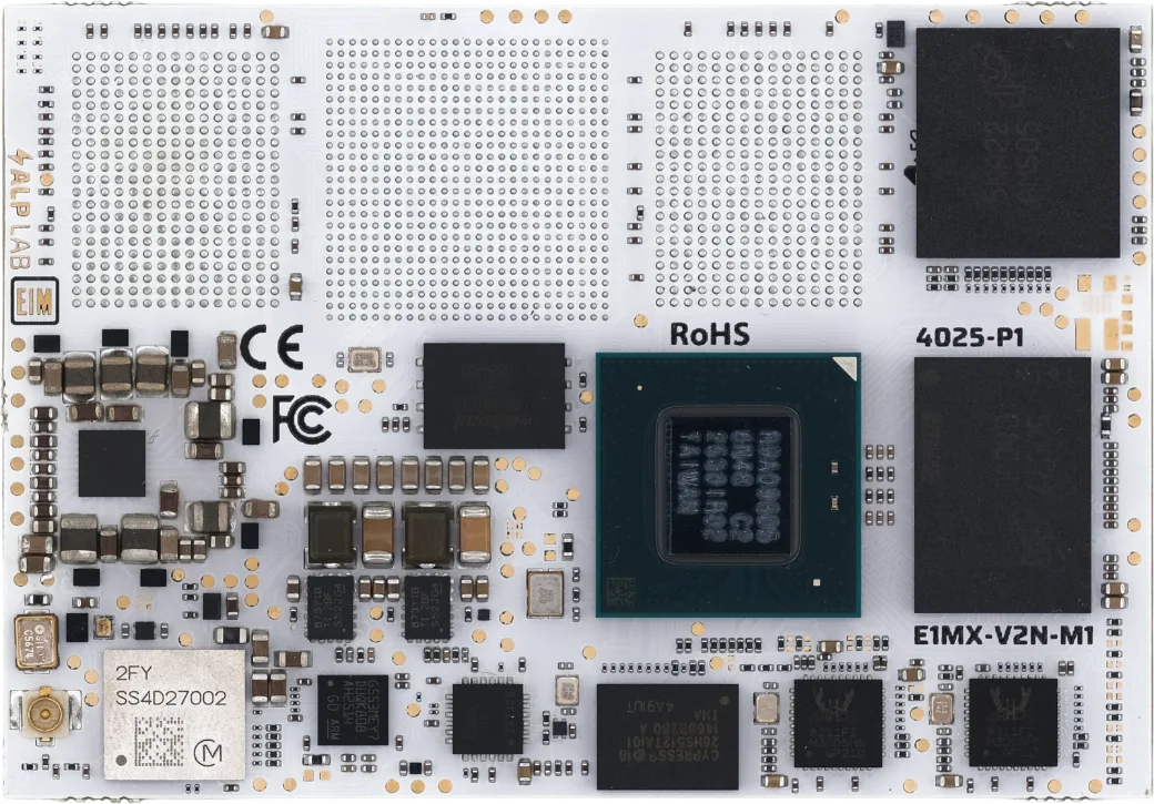
Module variants
Both SKUs share the same silicon + PCB. Pick by memory budget.
| SKU | Memory | Status |
|---|---|---|
E1M-V2N101 | 32 Gbit LPDDR4X + 32 Gbit eMMC | production |
E1M-V2N102 | 64 Gbit LPDDR4X + 64 Gbit eMMC | production |
At a glance
| Parameter | Value |
|---|---|
| Application core | Quad Arm Cortex-A55 @ 1.8 GHz |
| Real-time core | Arm Cortex-M33 |
| AI accelerator | Renesas DRP-AI3 |
| AI performance | 4 TOPS (dense) |
| Module dimensions | 65 × 45 × 5 mm |
| Form factor | E1M-X (45 × 65 mm), LGA |
| OS targets | Yocto Linux (A55) · Zephyr / bare-metal (M33) |
| Indicative price | $89 |
What's on the module
| Role | Part | Bus / signal | Driver |
|---|---|---|---|
| Application SoC | Renesas RZ/V2N (R9A09G056N44) | -- | (vendor HAL) |
| Companion supervisor MCU | GigaDevice GD32G553MEY7TR | SPI + I2C bridge | <alp/chips/gd32g553.h> |
| Primary PMIC | Qorvo ACT88760-120.E1 | I2C 0x25/0x26 | <alp/chips/act8760.h> |
| Secondary PMIC | Renesas DA9292 | I2C 0x1E | <alp/chips/da9292.h> |
| Clock generator | Renesas / IDT 5L35023B | I2C 0x68 | <alp/chips/clk_5l35023b.h> |
| RTC | Micro Crystal RV-3028-C7 | I2C 0x52 | <alp/chips/rv3028c7.h> |
| Temperature sensor | TI TMP112 | I2C 0x48 | <alp/chips/tmp112.h> |
| Secure element | Infineon OPTIGA Trust M | I2C 0x30 | <alp/chips/optiga_trust_m.h> (probe-only) |
| EEPROM (SoM manifest) | Onsemi N24S128 | I2C 0x50 | <alp/chips/eeprom_24c128.h> |
| Wi-Fi 6 + BLE 5.4 | Murata LBEE5HY2FY-922 | SDIO + UART + I2S | <alp/chips/murata_lbee5hy2fy.h> |
| Ethernet PHY ×2 | Realtek RTL8211FDI | RGMII + MDIO | <alp/chips/rtl8211fdi.h> |
| eMMC | (variant per SKU) | Renesas SD0 | Zephyr SD subsystem |
| NOR flash | (variant per SKU) | Renesas xSPI0 | Zephyr flash subsystem |
A fourth TPS628640 buck at 0x4D (a Renesas LPDDR4X rail) is an assembly option on this SKU — firmware treats a no-ACK there as a skip, not a failure.
:::note TMP112 address
The TMP112 sits at 0x48 (ADD0 strapped to GND, the chip default). Earlier revisions of this page and of the SDK metadata listed 0x40, which is outside the part's physically possible 0x48..0x4B strap range. The metadata is corrected; bench confirmation on silicon is still pending, so the SDK's bring-up example deliberately scans the whole strap range and reports what it finds.
:::
Processor architecture
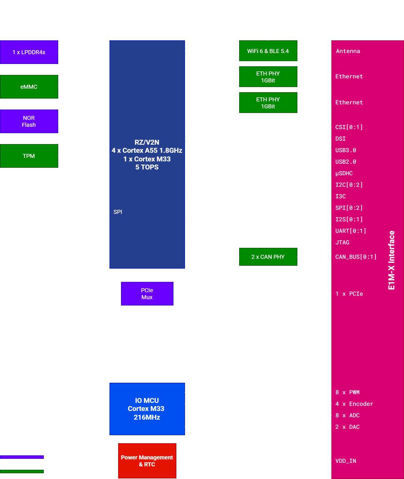
Application cores (Cortex-A55)
Four Cortex-A55 cores running at up to 1.8 GHz host a full Linux distribution (Yocto-built). They handle application logic, networking, display output, and pre/post-processing for AI pipelines.
Real-time core (Cortex-M33)
The Cortex-M33 subsystem operates independently and runs bare-metal or Zephyr firmware via the Alp SDK. It is ideal for:
- Sensor data acquisition with deterministic latency
- PWM and motor control
- Safety-critical tasks
DRP-AI3 accelerator
Renesas's DRP-AI3 provides 4 TOPS of dense inference performance. Models are deployed through the SDK's <alp/inference.h> dispatcher with the ALP_SDK_INFERENCE_DRPAI Kconfig. Model conversion uses the upstream DRP-AI Translator toolchain.
GD32 supervisor MCU
The V2N module's GD32G553 supervisor MCU owns all eight E1M PWM channels (PWM0..PWM7), the dual ADC/DAC bank, the Wi-Fi/BT REG_ON pins, the OPTIGA reset, and 18 IO routes to the E1M edge.
2026-05 hardware decision: GD32-only PWMs. The earlier "either GD32 or Renesas, picked SoM-wide via resistor strap" cross-source design was dropped — Renesas drives no PWMs on V2N. The resistor-strap selection is no longer applicable; there's nothing to switch between.
:::note Design against the E1M edge, not the module internals
The supervisor's own pin assignments are module-internal implementation detail and are deliberately not published. Your carrier design targets the E1M edge connector — that is the interface the lifecycle statement's form-fit-function guarantee covers across hardware revisions. Access the supervisor's peripherals through the portable <alp/*.h> surfaces, which stay stable even if the internal routing changes.
:::
Bridge-only peripheral classes
On V2N (and V2N-M1), five portable peripheral classes are served exclusively by the GD32 IO-MCU bridge. There is no native RZ/V2N path for any of them, and none is planned:
| Class | Portable API | Connector-position IDs |
|---|---|---|
adc | <alp/adc.h> | ALP_E1M_X_ADC0..ALP_E1M_X_ADC7 |
pwm | <alp/pwm.h> | ALP_E1M_X_PWM0..ALP_E1M_X_PWM7 |
dac | <alp/dac.h> | ALP_E1M_X_DAC0..ALP_E1M_X_DAC1 |
counter | <alp/counter.h> | — |
qenc (quadrature encoder) | <alp/counter.h> — alp_qenc_open() | ALP_E1M_X_ENC0..ALP_E1M_X_ENC3 |
The RZ/V2N SoC metadata has no dac key at all — the portable alp_dac surface exists on V2N solely because of the bridge.
Those IDs are always routed through the bridge. There is no fallback backend, because a "native" candidate has no pad to reach. If the bridge is unreachable, the portable alp_*_open() call fails rather than silently degrading:
| Condition | Result |
|---|---|
| Neither supervisor bus opening | ALP_ERR_NOT_READY |
| Supervisor mutex timeout | ALP_ERR_BUSY |
| Built without supervisor support | ALP_ERR_NOSUPPORT |
Two current limits, stated plainly:
- The bridge ADC path exposes no hardware oversampling or triggering. That is an SDK gap, not a bridge limitation.
counterset_alarmreturnsALP_ERR_NOSUPPORT— there is no interrupt line from the GD32 back to the Renesas SoC.
Host transports
The host driver speaks both transports:
- SPI fast path — Renesas SCI7 (Simple-SPI master) ↔ GD32 slave at up to 25 MHz, silicon-validated with a full-DMA slave data path on the GD32 side and a zero-interrupt polled engine on the host. Use for high-frequency telemetry and PWM updates. (A move to RSPI is planned for the next hardware revision.)
- I2C management path — on
BRD_I2C, GD32 at 7-bit0x70. Use when you're already onBRD_I2Cfor the PMIC fleet.
Current bridge firmware is v0.2.11, speaking wire protocol v0.9. The firmware release version and the wire-protocol version are independent axes: GET_VERSION returns the protocol triple, GET_BUILD_ID returns the firmware release plus its build SHA.
Protocol history since v0.6:
| Protocol | Adds |
|---|---|
| v0.7 | LINK_FEATURES negotiation with a STATUS_SEQ reply stamp that kills stale-reply hazards on the SPI link; OTA_BEGIN records the incoming image version into the A/B slot metadata |
| v0.8 | SE_RESET — host control of the on-module secure element's reset line |
| v0.9 | ADC oversample / resolution control, PWM center-aligned mode, and an ADC DSP chain with runtime dispatch — FAC-backed FIR/IIR filtering plus a hardware FFT spectrum path read back over ADC_SPECTRUM_READ |
Each of these is additive and backward-compatible by construction — an older host simply never sends the new opcodes, and v0.7's negotiated framing is byte-identical to v0.6 until LINK_FEATURES is agreed. Pre-1.0, though, the host driver and firmware still ship in lock-step on minor, not just major: a pre-production minor may revise a pre-production opcode's payload, and the major-only handshake cannot detect that. Don't mix host and bridge across minors.
Bridge firmware OTA
The bridge firmware is field-updatable over the link (OTA Path-A: chunked write → CRC-32 verify → commit, with rollback to the other bank). The host driver refuses to start an OTA session against a bridge advertising protocol minor < 6, before any erase or program — a pre-v0.6 bridge decodes the v0.6 chunk framing as image data and would be corrupted. OTA_BEGIN is non-blocking: it arms a background erase of the 236 KB slot and acks immediately rather than stalling the SPI reply. The bootloader orders both metadata records newest-first and falls back to an older bootable record if the newest fails validation.
Silicon status: boot-select, dual-bank erase, and the background-erase path are silicon-validated on the GD32. The bench evidence for the wider bridge suite (functional suite, HIL soak, A/B OTA end-to-end, analog loopback) was captured at firmware v0.2.9 / protocol v0.7.
For bench flashing there is an external-probe SWD path (J-Link primary) and a host bit-bang SWD path for recovery — see GD32 SWD Flash.
gd32g553_t bridge;
gd32g553_init(&bridge, spi, brd_i2c, GD32G553_BRIDGE_DEFAULT_I2C_ADDR);

uint32_t period_ns = 1000000u; // 1 kHz
uint32_t duty_ns   = 500000u;  // 50 %
gd32g553_pwm_set(&bridge, /* channel */ 0u, period_ns, duty_ns);
The wire protocol and bring-up flow are documented in the SDK repo at docs/gd32-bridge-protocol.md.
Dual Ethernet
Two RTL8211FDI gigabit PHYs sit on separate MDIO buses. The SDK's PHY driver takes function-pointer callbacks so it works against any MDIO controller, including bridge-side MDIO:
rtl8211fdi_t phy0;
rtl8211fdi_init(&phy0, /* phy_addr */ 0,
                my_mdio_read, my_mdio_write, mdio_dev);
rtl8211fdi_soft_reset(&phy0, 500000);
rtl8211fdi_restart_autoneg(&phy0);
How Ethernet is exposed
There is no <alp/ethernet.h> and no <alp/net.h> — Ethernet's data plane and its generic control plane sit deliberately outside the portable <alp/*> surface. Three layers carry it instead:
| Layer | On V2N |
|---|---|
| Compile-time capability | ALP_CAP_HW_ETHERNET |
| Form-factor port identity | ALP_E1M_X_ETH0, ALP_E1M_X_ETH1, with ALP_E1M_X_ETH_COUNT 2u |
| PHY chip driver | <alp/chips/rtl8211fdi.h> |
(The E1M form factor's equivalent identity is ALP_E1M_ETH0 with ALP_E1M_ETH_COUNT 1u.)
The RZ/V2N SoC metadata (renesas:rzv2n:n44, shared by V2N and V2N-M1) now reports an Ethernet count of 2. It previously read 0: a metadata-generator bug — the count matched only the key ethernet, while the source spells it ethernet_1g: 2. No hardware changed.
Debug console
The E1M-X spec (v1.2) routes the dedicated debug-console UART on two previously-reserved E1M-X pads:
| E1M-X pad | Signal |
|---|---|
AC62 | DBG_TX |
AD62 | DBG_RX |
The E1M (35 × 35 mm) form factor carries the same console at AD3 / AE3.
Getting started
- Mount the E1M-X V2N on a compatible board (E1M-X-EVK or custom).
- Flash the Yocto image to the A55 cluster (
MACHINE = e1m-v2n101-a55). - For M33 development, install the Alp SDK and drop a
board.yamlwithsom.sku: E1M-V2N101and acores.m33_sm:block — or pick one of the heterogeneous flagship examples that drives both halves from one file. - Build with
tan --project alp-sdk/examples/multicore/rpmsg-v2n build(heterogeneous) ortan --project alp-sdk/examples/v2n/v2n-gd32-bridge-ping build(M33-only).
M33 board target
The M33 system-manager board is alp_e1m_v2n101_m33_sm. Because RZ/V2N is a multi-cluster SoC (A55 + M33), a bare west build -b needs the fully-qualified identifier:
alp_e1m_v2n101_m33_sm/r9a09g056n48gbg/cm33
tan build derives the qualifiers from your board.yaml, so you never type the identifier there. Two details worth knowing:
- Zephyr models the die as the
n48gbgvariant even though the SoM carriesR9A09G056N44GBG. The n44/n48 delta is GPU / ISP / crypto fusing; the two are devicetree-identical for the M33 and its SPI / I2C. This is deliberate, not a typo. - The board is headless — the only console is the A55's.
CONFIG_CONSOLEis off by default, because the M33'ssci0is not wired as a console here and opening it faults on the floating RX line. For M33-side visibility, use the RAM console the SDK's simulator diagnostics stream instead.
The V2N-M1 SKU has its own parallel target, alp_e1m_v2m101_m33_sm. Both board definitions are generated from the SoM metadata rather than hand-authored.
Resources
- Firmware quickstart — V2N-specific patterns
<alp/inference.h>— DRP-AI3 dispatcher- Chip catalogue — every on-module driver
- E1M-X EVK — reference board
- Industrial inquiries